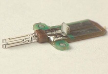
Tips Nano AFMプローブ
AFM Standard/原子間力顕微鏡・AFMカンチレバー
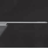
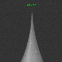
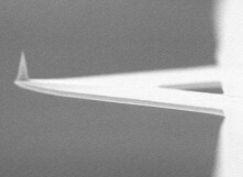
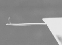
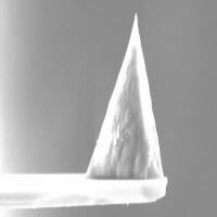
The cantilever is a key element of any scanning probe microscope, the properties and quality of which depends on the successful operation of the microscope in General. This is the basic measuring element of many types of probe microscopes. The right choice of the cantilever is one of the most important conditions for obtaining good AFM images. The most important component of AFM (Atomic force microscope) are the scanning probes of the cantilevers. The cantilever is a flexible beam (175х40х4 µm — average data) with a certain stiffness coefficient k (10-3 – 10 N/m), which is a micro needle.
-Semicontact-/AFMセミコンタクトプローブ
Standard Tapping / Noncontact AFM probes with wide range of resonant frequencies and force constants.
NSG01
Product Description
High Resolution Silicon AFM Cantilevers NSG01 series.are designed for Semicontact ( Intermittent ), Noncontact applications. Typical Resonant Frequency 150 kHz (guaranteed range 87-230kHz), Typical Force Constant 5.1 N/m (guaranteed range 1.45-15.1N/m). Cantilever has Au reflective side coating to increase laser signal. Probes are also available with no coating as well as with conductive tip coating.
NSG03
Product Description
High Resolution Silicon AFM Cantilevers NSG03 series are designed for Semicontact ( Intermittent ), Noncontact applications. Typical Resonant Frequency 90 kHz (guaranteed range 47-150kHz), Typical Force Constant 1.74 N/m (guaranteed range 0.35-6.1N/m). Cantilever has Au reflective side coating to increase laser signal.Probes are also available with no coating as well as with conductive tip coating.
NSG30
Product Description
High Resolution Silicon AFM Cantilevers NSG30 series.are designed for Semicontact ( Intermittent ), Noncontact applications. Typical Resonant Frequency 320 kHz (guaranteed range 240-440 kHz), Typical Force Constant 40 N/m (guaranteed range 22-100 N/m). Cantilever has Au reflective side coating to increase laser signal. Probes are also available with no coating as well as with conductive tip coating.
VIT_P/IR

Product Description
TOP VISUAL High Resolution Semicontact / Noncontact Silicon AFM Cantilevers VIT_P/IR series are specially designed for tip or laser spot precise positioning over the point of interest. Typical Resonant Frequency 300 kHz (guaranteed range 200-400 kHz), Typical Force Constant 50 N/m (guaranteed range 25-95 N/m). Cantilevers have Au reflective coating. Probes are also available with no coating as well as with conductive tip coating.
HA_HR

Product Description
High Resolution High Resonant Frequency AFM Cantilevers HA_FM series are designed for Semicontact ( Intermittent ), Noncontact applications. Each probe has 2 rectangular cantilevers.Typical Resonant Frequency 114kHz / 77kHz (dispersion ±10%). Typical Force Constant 12N/m / 3.5N/m (dispersion ±20%). Cantilever has Au reflective side coating to increase laser signal. Probes are also available with no coating as well as with conductive tip coating.
HA_FM
Product Description
High Resolution High Resonant Frequency AFM Cantilevers HA_FM series are designed for Semicontact ( Intermittent ), Noncontact applications. Each probe has 2 rectangular cantilevers.Typical Resonant Frequency 114kHz / 77kHz (dispersion ±10%). Typical Force Constant 12N/m / 3.5N/m (dispersion ±20%). Cantilever has Au reflective side coating to increase laser signal. Probes are also available with no coating as well as with conductive tip coating.
HA_CNC
Product Description
High Resolution High Accuracy AFM Cantilevers HA_CNC series are designed for Semicontact ( Intermittent ), Noncontact applications. Each probe has 2 rectangular cantilevers.Typical Resonant Frequency 66kHz / 46kHz (dispersion ±10%). Typical Force Constant 1.5N/m / 1.0N/m (dispersion ±20%). Cantilever has Au reflective side coating to increase laser signal. Probes are also available with no coating as well as with conductive tip coating.
NSG10
Product Description
High Resolution Silicon AFM Cantilevers NSG10 series.are designed for Semicontact ( Intermittent ), Noncontact applications. Typical Resonant Frequency 240 kHz (guaranteed range 140-390kHz), Typical Force Constant 11.8 N/m (guaranteed range 3,1-37,6N/m). Cantilever has Au reflective side coating to increase laser signal.Probes are also available with no coating as well as with conductive tip coating.
VIT_P
Product Description
TOP VISUAL High Resolution Semicontact / Noncontact Silicon AFM Cantilevers VIT_P series are specially designed for tip or laser spot precise positioning over the point of interest. Typical Resonant Frequency 300 kHz (guaranteed range 200-400 kHz), Typical Force Constant 50 N/m (guaranteed range 25-95 N/m). Cantilevers have no coating. Probes are also available with Au reflective coating as well as with conductive tip coating.
HA_NC
Product Description
High Resolution High Accuracy AFM Cantilevers HA_NC series are designed for Semicontact ( Intermittent ), Noncontact applications. Each probe has 2 rectangular cantilevers.Typical Resonant Frequency 235kHz / 140kHz (dispersion ±10%). Typical Force Constant 12N/m / 3.5N/m (dispersion ±20%). Cantilever has Au reflective side coating to increase laser signal. Probes are also available with no coating as well as with conductive tip coating.
-Contact-/AFMコンタクトプローブ
Standard Contact-Mode AFM probes.
CSG30
Product Description
High Resolution Silicon AFM Cantilevers CSG30 series are designed for Contact/noncontact applications. Typical Resonant Frequency 48 kHz (guaranteed range 26-76kHz), Typical Force Constant 0,6 N/m (guaranteed range 0,13-2N/m). Cantilever has Au reflective side coating to increase laser signal. Probes are also available with no coating as well as with conductive tip coating.
CSG01
Product Description
High Resolution Silicon AFM Cantilevers CSG01 series are designed for Contact applications. Typical Resonant Frequency 9,8 kHz (guaranteed range 4-17kHz), Typical Force Constant 0,03 N/m (guaranteed range 0,003-0,13N/m). Cantilever has Au reflective side coating to increase laser signal. Probes are also available with no coating as well as with conductive tip coating.
CSG11

Product Description
Contact Mode AFM probes CSG11 series. Each chip has 2 rectangular cantilevers, typical resonant frequency 21kHz/ 11kHz, force constant 0.1N/m / 0.05N/m. Cantilever has Au reflective side coating to increase laser signal.
VIT_P_C-A
Product Description
TOP VISUAL High Resolution Contact Silicon AFM Cantilevers VIT_P_C-A series are specially designed for tip or laser spot precise positioning over the point of interest. Typical Resonant Frequency 16 kHz (guaranteed range 8-25 kHz), Typical Force Constant 0.3 N/m (guaranteed range 0.06-1N/m). Cantilevers have Al reflective coating.
HA_C
Product Description
High Resolution AFM Cantilevers HA_C series are designed for Contact mode and Lateral Force Mode applications. Each probe has 2 rectangular cantilevers.Typical Resonant Frequency 37kHz / 19kHz (dispersion ±10%). Typical Force Constant 0.65N/m / 0.26N/m (dispersion ±20%). Cantilever has Au reflective side coating to increase laser signal. Probes are also available with no coating as well as with conductive tip coating.
CSG10
Product Description
High Resolution Silicon AFM Cantilevers CSG10 series are designed for Contact applications. Typical Resonant Frequency 22 kHz (guaranteed range 8-39kHz), Typical Force Constant 0,11 N/m (guaranteed range 0,01-0,5N/m). Cantilever has Au reflective side coating to increase laser signal. Probes are also available with no coating as well as with conductive tip coating.
-Force Modulation-/フォースモジュレーション顕微鏡モードAFMプローブ
Multi-functional AFM probes.
FMG01
Product Description
High Resolution Silicon AFM Cantilevers FMG01 series are designed for Force Modulation applications. Typical Resonant Frequency 60 kHz (guaranteed range 40-96kHz), Typical Force Constant 3 N/m (guaranteed range 1-5N/m). Cantilever has Au reflective side coating to increase laser signal. Probes are also available with no coating as well as with conductive tip coating.
HA_FM
Product Description
High Resolution High Resonant Frequency AFM Cantilevers HA_FM series are designed for Semicontact ( Intermittent ), Noncontact applications. Each probe has 2 rectangular cantilevers.Typical Resonant Frequency 114kHz / 77kHz (dispersion ±10%). Typical Force Constant 12N/m / 3.5N/m (dispersion ±20%). Cantilever has Au reflective side coating to increase laser signal. Probes are also available with no coating as well as with conductive tip coating.
-Conductive-/コンダクティブAFMプローブ
Electrical measurements AFM probes.
HA_FMHA_HR/W2C+
Product Description
High Resolution High Resonant Frequency AFM Cantilevers HA_HR/W2C+ series are designed for Semicontact ( Intermittent ), Noncontact and electrical applications (SKM, SCM, SRIM, EFM, LAO Lithography).
Hard and stable coating provides long time perfomance in all electrical modes. Specially doped W2C+ coating allows to avoid probes from oxidation, extends probe lifetime and makes it possible to operate at high-humidity conditions.
Each probe has 2 rectangular cantilevers.Typical Resonant Frequency 380kHz / 230kHz (dispersion ±10%), Typical Force Constant 34N/m / 17N/m (dispersion ±20%). Cantilever has Au reflective and W2C tip side coatings. Probes are also available without tip coating.
NSG30/Au
Product Description
High Resolution Silicon AFM Cantilevers NSG30/Au series are designed for Conductive applications. Typical Resonant Frequency 320 kHz (guaranteed range 240-440kHz), Typical Force Constant 40 N/m (guaranteed range 22-100N/m). Cantilever has Au reflective side coating to increase laser signal.
NSG03/Au
Product Description
High Resolution Silicon AFM Cantilevers NSG03/Au series are designed for Conductive applications. Typical Resonant Frequency 90 kHz (guaranteed range 47-150kHz), Typical Force Constant 1,74 N/m (guaranteed range 0,35-6,1N/m). Cantilever has Au reflective side coating to increase laser signal.
CSG01/Au
Product Description
High Resolution Silicon AFM Cantilevers CSG01/Au series are designed for Conductive applications. Typical Resonant Frequency 9,8 kHz (guaranteed range 4-17kHz), Typical Force Constant 0,03 N/m (guaranteed range 0,003-0,13N/m). Cantilever has Au reflective side coating to increase laser signal.
FMG01/Au
Product Description
High Resolution Silicon AFM Cantilevers FMG01/Au series are designed for Conductive applications. Typical Resonant Frequency 60 kHz (guaranteed range 40-96kHz), Typical Force Constant 3 N/m (guaranteed range 1-5N/m). Cantilever has Au reflective side coating to increase laser signal.
CSG01/Pt
Product Description
High Resolution Silicon AFM Cantilevers CSG01/Pt series are designed for Conductive applications. Typical Resonant Frequency 9,8 kHz (guaranteed range 4-17kHz), Typical Force Constant 0,03 N/m (guaranteed range 0,003-0,13N/m). Cantilever has PtIr tip and reflective sides coating.
NSG10/Au
Product Description
High Resolution Silicon AFM Cantilevers NSG10/Au series are designed for Conductive applications. Typical Resonant Frequency 240 kHz (guaranteed range 140-390kHz), Typical Force Constant 11,8 N/m (guaranteed range 3,1-37,6N/m). Cantilever has Au reflective side coating to increase laser signal.
NSG03/Pt
Product Description
High Resolution Silicon AFM Cantilevers NSG03/Pt series are designed for Conductive applications. Typical Resonant Frequency 90 kHz (guaranteed range 47-150kHz), Typical Force Constant 1,74 N/m (guaranteed range 0,35-6,1N/m). Cantilever has PtIr tip and reflective sides coating.
NSG30/Pt
Product Description
High Resolution Silicon AFM Cantilevers NSG30/Pt series are designed for Conductive applications. Typical Resonant Frequency 320 kHz (guaranteed range 240-440kHz), Typical Force Constant 40 N/m (guaranteed range 22-100N/m). Cantilever has PtIr tip and reflective sides coating.
CSG10/Au
Product Description
High Resolution Silicon AFM Cantilevers CSG10/Au series are designed for Conductive applications. Typical Resonant Frequency 22 kHz (guaranteed range 8-39kHz), Typical Force Constant 0,11 N/m (guaranteed range 0,01-0,5N/m). Cantilever has PtIr reflective side coating to increase laser signal.
NSG01/Au
Product Description
High Resolution Silicon AFM Cantilevers NSG01/Au series are designed for Conductive applications. Typical Resonant Frequency 150 kHz (guaranteed range 87-230kHz), Typical Force Constant 5,1 N/m (guaranteed range 1,45-15.1N/m). Cantilever has Au reflective side coating to increase laser signal.
CSG10/Pt
Product Description
High Resolution Silicon AFM Cantilevers CSG10/Pt series are designed for Conductive applications. Typical Resonant Frequency 22 kHz (guaranteed range 8-39kHz), Typical Force Constant 0,11 N/m (guaranteed range 0,01-0,5N/m). Cantilever has PtIr tip and reflective sides coating.
NSG10/Pt
Product Description
High Resolution Silicon AFM Cantilevers NSG10/Pt series are designed for Conductive applications. Typical Resonant Frequency 240 kHz (guaranteed range 140-390kHz), Typical Force Constant 11,8 N/m (guaranteed range 3,1-37,6N/m). Cantilever has PtIr tip and reflective sides coating.
NSG01/Pt
Product Description
High Resolution Silicon AFM Cantilevers NSG01/Pt series are designed for Conductive applications. Typical Resonant Frequency 150 kHz (guaranteed range 87-230kHz), Typical Force Constant 5.1 N/m (guaranteed range 1,45-15,1N/m). Cantilever has PtIr tip and reflective sides coating.
FMG01/Pt
Product Description
High Resolution Silicon AFM Cantilevers FMG01/Pt series are designed for Conductive applications. Typical Resonant Frequency 60 kHz (range 35-90kHz), Typical Force Constant 1.6 N/m (guaranteed range 0.8-3.0N/m). Cantilever has PtIr tip and reflective sides coating.
CSG01/TiN
Product Description
High Resolution Silicon AFM Cantilevers CSG01/TiN series are designed for Conductive applications. Typical Resonant Frequency 9,8 kHz (guaranteed range 4-17kHz), Typical Force Constant 0,03 N/m (guaranteed range 0,003-0,13N/m). Cantilever has Au reflective side coating to increase laser signal.
NSG03n/TiN
Product Description
Noncontact/Semicontact Conductive Probes NSG03n/TiN series with TiN tips coating. Resonant frequency 62-123 kHz, force constant 0,4-2,7 N/m. Cantilever has Au reflective side coating to increase laser signal.
NSG01n/TiN
Product Description
Noncontact/Semicontact Conductive Probes NSG01n/TiN series with TiN tips coating Resonant frequency 115-190 kHz, force constant 2,5-10 N/m. Cantilever has Au reflective side coating to increase laser signal.
NSG10n/TiN
Product Description
Noncontact/Semicontact Conductive Probes NSG10n/TiN series with TiN tips coating. Resonant frequency 190-325 kHz, force constant 5,5-22.5 N/m. Cantilever has Au reflective side coating to increase laser signal. In comparison with NSG10/TiN probes NSG10n/Tin probes have bigger chip size, slight difference in lever parameters and keep stable condutivity on freshly cleaved HOPG till applied voltage ± 3V.
HA_FM/Au
Product Description
High Resolution High Resonant Frequency AFM Cantilevers HA_FM/Au series are designed for Semicontact ( Intermittent ), Noncontact and electrical applications (SKM, SCM, SRIM, EFM, LAO Lithography). Each probe has 2 rectangular cantilevers.Typical Resonant Frequency 114kHz / 77kHz (dispersion ±10%). Typical Force Constant 12N/m / 3.5N/m (dispersion ±20%). Cantilever has Au tip and reflective side coatings. Probes are also available without tip coating.
HA_C/Pt
Product Description
High Resolution AFM Cantilevers HA_C/Pt series are designed for Contact, Lateral Force and electrical applications. Each probe has 2 rectangular cantilevers. Typical Resonant Frequency 37kHz / 19kHz (dispersion ±10%). Typical Force Constant 0.65N/m / 0.26N/m (dispersion ±20%). Cantilever has Au reflective and Pt tip side coatings. Probes are also available with no tip coating.
HA_HR/Pt
Product Description
High Resolution High Resonant Frequency AFM Cantilevers HA_HR/Pt series are designed for Semicontact ( Intermittent ), Noncontact and electrical applications (SKM, SCM, SRIM, EFM, LAO Lithography). Each probe has 2 rectangular cantilevers.Typical Resonant Frequency 380kHz / 230kHz (dispersion ±10%), Typical Force Constant 34N/m / 17N/m (dispersion ±20%). Cantilever has Au reflective and Pt tip side coatings. Probes are also available without tip coating.
HA_NC/Pt
Product Description
High Resolution High Accuracy AFM Cantilevers HA_NC/Pt series are designed for Semicontact ( Intermittent ), Noncontact and electrical applications (SKM, SCM, SRIM, EFM, LAO Lithography). Each probe has 2 rectangular cantilevers.Typical Resonant Frequency 235kHz / 140kHz (dispersion ±10%). Typical Force Constant 12N/m / 3.5N/m (dispersion ±20%). Cantilever has Au reflective and Pt tip side coatings. Probes are also available without tip coating.
-Magnetic-/マグネティックAFMプローブ
High resolution long lifetime magnetic probes. These probes allow to carry out both ordinary measurements with high accuracy and resolution to 20-30nm (MFM01, MFM10) and the measurements with special requirements such as the experiments in high external fields (MFM_HC) and imaging low coercive magnetic samples (MFM_LM).
MFM10
Product Description
High Resolution Silicon AFM Cantilevers MFM10 and MFM01 series.are specially designed for work in magnetic AFM mode (MFM). Due to optimized coating thickness these probes suit for different magnetic samples and are recommended for initial measurements of new samples. Upon reviewing the results you can take a decision if the MFM coating used is the appropriate one or it is better to try another type of magnetic coating. Due to special defensive layers which prevent the ferromagnetic tip coating from oxidizing, all MFM probes have a long shelf life, and the small tip curvature radius enables you to obtain good high resolution images. Typical Resonant Frequency of the probes 150 kHz (guaranteed range 87-230kHz), typical Force Constant 5.1 N/m (guaranteed range 1.45-15.1N/m). Cantilever has Al reflective side coating to increase laser signal.
HA_FM/CoFe
Product Description
High Resolution High Resonant Frequency AFM Cantilevers HA_FM series are designed for Magnetic, Semicontact ( Intermittent ), Noncontact applications. Each probe has 2 rectangular cantilevers.Typical Resonant Frequency 114kHz / 77kHz (dispersion ±10%). Typical Force Constant 12N/m / 3.5N/m (dispersion ±20%). Cantilever has Au reflective and CoFe tip side coatings. Probes are also available without tip coating. Guaranteed lifetime is within 3 months.
MFM_LM
Product Description
Low Moment Magnetic High Resolution Silicon AFM Cantilevers MFM_LM series.are specially designed for work in magnetic AFM mode (MFM) with low coercive magnetic samples. MFM_LM probes have thinner magnetic coating than ordinary magnetic tips. So, such low coercive magnetic samples as iron garnet films, ordered array of interaсting Co particles, ordered array of vertically magnetized 35nm CoPt dots can be measured (see MFM images obtained by MFM_LM probes in the pictures bar). Thanks to their own low magnetic fields low moment MFM_LM probes allow to decrease the probe influence on the researched sample while scanning. Due to special defensive layers which prevent the ferromagnetic tip coating from oxidizing, all MFM probes have a long shelf life, and the small tip curvature radius enables you to obtain good high resolution images. Typical Resonant Frequency of the probes 70 kHz (guaranteed range 47-90kHz), typical Force Constant 3N/m (guaranteed range 1-5N/m). Cantilever has Al reflective side coating to increase laser signal.
MFM01
Product Description
High Resolution Silicon AFM Cantilevers MFM01 series.are specially designed for work in magnetic AFM mode (MFM). Due to optimized coating thickness these probes suit for different magnetic samples and are recommended for initial measurements of new samples. Upon reviewing the results you can take a decision if the MFM coating used is the appropriate one or it is better to try another type of magnetic coating. Due to special defensive layers which prevent the ferromagnetic tip coating from oxidizing, all MFM probes have a long shelf life, and the small tip curvature radius enables you to obtain good high resolution images. Typical Resonant Frequency of the probes 70 kHz (guaranteed range 47-90kHz), typical Force Constant 3N/m (guaranteed range 1-5N/m). Cantilever has Al reflective side coating to increase laser signal.
-Tipless-/チップレスプローブ
For chemical modifications, gluing spheres, etc.
NSG11/tipless
Product Description
Tipless Semicontact / Noncontact Conductive Probes NSG11/tipless series. Each chip has 2 rectangular cantilevers, typical resonant frequency 255kHz/ 150kHz, force constant 11.5N/m / 5,5N/m. Cantilevers has Au reflective side coating to increase laser signal.
HA_C/tipless
Product Description
Tipless High Accuracy AFM Cantilevers HA_C series are designed for Contact mode and Lateral Force Mode applications. Each probe has 2 rectangular cantilevers.Typical Resonant Frequency 37kHz / 19kHz (dispersion ±10%). Typical Force Constant 0.65N/m / 0.26N/m (dispersion ±20%). Cantilever has Au reflective side coating to increase laser signal.
-Cantilever Sets-AFMカンチレバーサンプルキット
New convenient format for probe puchasing. Cantilever sets which include different probe series for research of different samples by various AFM modes.
MIX_GL/50
Product Description
Personal Mixed Cantilever Set of 50 pieces GOLDEN probes is completed in accordance with customer’s needs.
Set can include any probes from the list:
・with Au reflective coating and no tip coating
NSG30, NSG10, NSG03, FMG01, CSG10, CSG01
・with Pt tips and reflective coating
NSG30/Pt, NSG10/Pt, NSG01/Pt, NSG03/Pt, FMG01/Pt, CSG10/Pt, CSG01/Pt
・with Au tip and reflective coating
NSG30/Au, NSG10/Au, NSG01/Au, NSG03/Au, FMG01/Au, CSG10/Au, CSG01/Au.
MIX_ET/50
Product Description
Personal Mixed Cantilever Set of 50 pieces ETALON probes is completed in accordance with customer’s needs.
Set can include any probes from the list:
・with Au reflective coating
HA_NC, HA_HR, HA_FM, HA_CNC, HA_C
・with Au reflective and Pt tip coating
HA_NC/Pt, HA_HR/Pt, HA_FM/Pt, HA_CNC/Pt, HA_C/Pt
・with Au tip and reflective coating
HA_NC/Au, HA_HR/Au, HA_C/Au
・with Au reflective and W2C tip coating
HA_HR/W2C, HA_NC/W2C.
MSSET/50
Product Description
MSSET/50 consists of 50 AFM probes:
・10 chips – for contact AFM;
・25 chips – for intermittent contact AFM;
・5 chips – for SSRM;
・5 chips – for SKM/SCM;
・5 chips – for MFM.
MFMSET/15
Product Description
Set of 15 High Resolution long lifetime magnetic probes.
MFMSET/15 consists of:
MFM01 – 5 probes
MFM10 – 5 probes
MFM_LM – 5 probes.
Set is intended for MFM measurements of different magnetic samples to find the best probes parameters for better imaging.
Due to special defensive layers which prevent the ferromagnetic tip coating from oxidizing, all MFM probes have a long shelf life, and the small tip curvature radius enables you to obtain good high resolution images.
Resonant Frequency:
MFM01, MFM_LM – 70 kHz (guaranteed range 47-90kHz),
MFM10 – 150 kHz (guaranteed range 87-230kHz),
Force Constant:
MFM01, MFM_LM – 3 N/m (guaranteed range 1-5 N/m).
MFM10 – 5.1 N/m (guaranteed range 1.45-15.1N/m).
Detailed specification see using the links: MFM01, MFM10, MFM_LM.
Cantilevers has Al reflective side coating to increase laser signal.
UNISET/50
Product Description
Advanced UNISET/50 consists of:
・10 probes for noncontact/semicontact modes – NSG10
・10 probes for force modulation mode – FMG01
・10 probes for contact mode – CSG10
・5 probes for EFM, SCM, SKM modes – NSG01/Pt
・5 probes for SRM – CSG10/Pt
・5 probes with stable and nondestructive diamond like conductive coating for LAO Lithogpaphy and other conductive modes – DCP20
・5 probes with high resolution long lifetime magnetic coating for MFM – MFM01
The probe complectation can be different upon customers’ request.
MSSET/200
Product Description
MSSET/200 consists of 50 AFM probes:
・50 chips – for contact AFM;
・100 chips – for intermittent contact AFM;
・20 chips – for SSRM;
・25 chips – for SKM/SCM;
・5 chips – for MFM.
UNISET/25
Product Description
UNISET/25 consists of:
・5 probes for noncontact/semicontact modes – NSG30
・5 probes for contact modes – CSG10
・5 probes for PFM – FMG01/Pt
・5 probes for SRM – CSG10/Au
・5 probes for EFM, SCM, SKM – DCP01
The probe complectation can be different upon customers’ request.
AFM Special
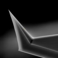
-High Aspect Ratio-/高アスペクト比プローブ
Whisker probe is an indispensable instrument for studying surfaces of unusual profile with narrow gaps.
Standard cantilevers fail to investigate such objects with the necessary precision.
CSC05
Product Description
Whisker Type High Aspect Ration Silicon AFM Cantilevers CSC05 series for Contact applications. Typical Resonant Frequency 22 kHz (guaranteed range 8-39kHz), Typical Force Constant 0.11 N/m (guaranteed range 0.01-0.5N/m). Cantilever has Au reflective side coating to increase laser signal.
Whisker probe is an indispensable instrument for studying surfaces of unusual profile with narrow gaps. Standard cantilevers fail to investigate such objects with the necessary precision.
Whisker probes differ from any standard ones by having long slim "whisker" at the very end of the tip. It is possible “whisker” to be grown at any angle to the silicon tip axis for being perpendicular to the investigated surface.
As standard product we offer two variants of inclination angle - 10 and 20 degrees. At customer's request any angle can be grown.
Probes are packed in boxes with 5 pieces.
NSC05
Product Description
Whisker Type High Aspect Ration Silicon AFM Cantilevers NSC05 series for Semicontact ( Intermittent ), Noncontact applications. Typical Resonant Frequency 240 kHz (guaranteed range 140-390kHz), Typical Force Constant 11.8 N/m (guaranteed range 3,1-37,6N/m). Cantilever has Au reflective side coating to increase laser signal.
Whisker probe is an indispensable instrument for studying surfaces of unusual profile with narrow gaps. Standard cantilevers fail to investigate such objects with the necessary precision.
Whisker probes differ from any standard ones by having long slim "whisker" at the very end of the tip. It is possible “whisker” to be grown at any angle to the silicon tip axis for being perpendicular to the investigated surface.
As standard product we offer two variants of inclination angle - 10 and 20 degrees. At customer's request any angle can be grown.
Probes are packed in boxes with 5 pieces.
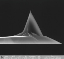
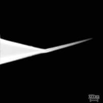
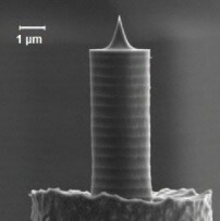
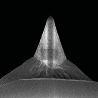
-Super Sharp-
Super sharp silicon probes and diamond-like carbon DLC tips with typical curvature radius 1-2nm are extremely useful for obtaining high resolution of nanostructures. DLC tips have very long lifetime due to the high material durability.
NSG10_DLC
Product Description
Super Sharp Diamond-Like Carbon (DLC) tips with typical curvature radius 1nm grown on the probe series NSG10, resonance frequency 255 kHz, force constant11.5 N/m.
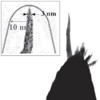
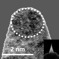
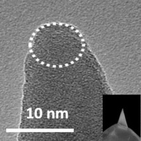
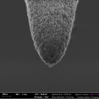
Super sharp diamond-like carbon (DLC) tips* with typical curvature radius 1nm are extremely useful for obtaining high resolution imaging on objects with sizes of several nanometers. DLC tips have very long lifetime due to the high material durability.
DLC tips can be grown on any standard probe series.
To guarantee 20nm working length of DLC tips TEM is used. 10% from total number of probes in the batch are selected for testing. At least 80% of those probes should have the only DLC tip which lengh is exceeded by 20nm others DLC tips on the same probe. In this case the whole batch is considered as passed the TEM test. On the surfaces with roughness bigger than 20nm double images are possible.
NSG01_DLC
Product Description
Super Sharp Diamond-Like Carbon (DLC) tips with typical curvature radius 1nm grown on the probe series NSG01, resonance frequency 150 kHz, force constant 5.5 N/m.
Super sharp diamond-like carbon (DLC) tips* with typical curvature radius 1nm are extremely useful for obtaining high resolution imaging on objects with sizes of several nanometers. DLC tips have very long lifetime due to the high material durability.
DLC tips can be grown on any standard probe series.
To guarantee 20nm working length of DLC tips TEM is used. 10% from total number of probes in the batch are selected for testing. At least 80% of those probes should have the only DLC tip which lengh is exceeded by 20nm others DLC tips on the same probe. In this case the whole batch is considered as passed the TEM test. On the surfaces with roughness bigger than 20nm double images are possible.
FMG01_SS
Product Description
Super Sharp High Resolution Silicon AFM Cantilevers FMG01_SS series are designed for Force Modulation applications. Typical Resonant Frequency 60 kHz (guaranteed range 40-96kHz), Typical Force Constant 3 N/m (guaranteed range 1-5N/m). Typical tip curvature radius is 2nm.
Using the probes with sharpened tips you will be able to increase resolution of the obtained images especially on objects with typical sizes of several nanometers.
Cantilever has Al reflective side coating to increase laser signal.
Probes are packed in boxes with 5 pieces.
Cantilever has Au reflective side coating to increase laser signal.
CSG10_SS
Product Description
Super Sharp High Resolution Silicon AFM Cantilevers CSG10_SS series are designed for Contact applications. Typical Resonant Frequency 22 kHz (guaranteed range 8-39kHz), Typical Force Constant 0,11 N/m (guaranteed range 0,01-0,5N/m). Typical tip curvature radius is 2nm.
Using the probes with sharpened tips you will be able to increase resolution of the obtained images especially on objects with typical sizes of several nanometers.
Cantilever has Al reflective side coating to increase laser signal.
Probes are packed in boxes with 5 pieces.
NSG30_SS
Product Description
Super Sharp High Resolution Silicon AFM Cantilevers NSG30_SS series are designed for Semicontact ( Intermittent ), Noncontact applications. Typical Resonant Frequency 320 kHz (guaranteed range 240-440 kHz), Typical Force Constant 40 N/m (guaranteed range 22-100 N/m). Typical tip curvature radius is 2nm.
Using the probes with sharpened tips you will be able to increase resolution of the obtained images especially on objects with typical sizes of several nanometers.
Cantilever has Al reflective side coating to increase laser signal.
Probes are packed in boxes with 5 pieces.
-Diamond Coated-
Diamond Coated Probes are the best choice for any kind of long-term electrical characterizations. Stable and nondestructive, wear resistant probes with diamond coating allow you to make as many images as you want.
DCP01

Product Description
Diamond Like Coated Conductive Probes DCP01 series are The best choice for any kind of long-term electrical characterizations. Stable and nondestructive, wear resistant probes with conductive diamond-like coating allow you to make as many images as you want. Resonant frequency 115-190 kHz, force constant 2,5-10 N/m. Cantilever has Au reflective side coating to increase laser signal.
DCP10

Product Description
Diamond Coated Conductive Probes DCP10 series are the best choice for any kind of long-term electrical characterizations. Stable and nondestructive, wear resistant probes with conductive diamond-like coating allow you to make as many images as you want. Resonant frequency 190-325 kHz, force constant 5,5-22.5 N/m. Cantilever has Au reflective side coating to increase laser signal.
DCP20
Product Description
Diamond Coated Conductive Probes DCP20 series with triangular cantilever are the best choice for any kind of long-term electrical characterizations. Stable and nondestructive, wear resistant probes with conductive diamond-like coating allow you to make as many images as you want. Resonant frequency 260-630 kHz, force constant 28-91 N/m. Cantilever has Au reflective side coating to increase laser signal.
DCP11
Product Description
Diamond Coated Conductive Probes DCP11 series are the best choice for any kind of long-term electrical characterizations. Stable and nondestructive, wear resistant probes with conductive diamond-like coating allow you to make as many images as you want. Each chip has 2 rectangular cantilevers, typical resonant frequency 255kHz/ 150kHz, force constant 11.5N/m / 5,5N/m, Au reflective coating. Cantilever has Au reflective side coating to increase laser signal.
HA_FM_DCP
Product Description
Diamond Coated High Resolution AFM Cantilevers HA_FM_DCP series are the best are for any kind of long-term measurement. Stable and nondestructive, wear resistant probes with diamond coating allow you to make as many images as you want. Each probe has 2 rectangular cantilevers.Typical Resonant Frequency 157kHz / 112kHz (dispersion ±10%). Typical Force Constant 14.5N/m / 8.3N/m (dispersion ±20%). Cantilever has Au reflective side coating to increase laser signal.
HA_C_DCP

Product Description
Diamond coated High Resolution AFM Cantilevers HA_C_DCP series are the best are for any kind of long-term measurement. Stable and nondestructive, wear resistant probes with diamond coating allow you to make as many images as you want. Each probe has 2 rectangular cantilevers. Typical Resonant Frequency 48kHz / 26kHz (dispersion ±10%). Typical Force Constant 1.4N/m / 0.7N/m (dispersion ±20%). Cantilever has Au reflective coating.
HA_HR_DCP
Product Description
Diamond coated High Resolution AFM Cantilevers HA_HR_DCP series are the best are for any kind of long-term measurement. Stable and nondestructive, wear resistant probes with diamond coating allow you to make as many images as you want. Each probe has 2 rectangular cantilevers. Typical Resonant Frequency 580kHz / 330kHz (dispersion ±10%). Typical Force Constant 85N/m / 35N/m (dispersion ±20%). Cantilever has Au reflective coating.
-Top Visual-
The best choice for the applications where the tip has to be placed exactly on the point of interest and/or has to be visible for Nanomanipulation.
VIT_P/IR

Product Description
TOP VISUAL High Resolution Semicontact / Noncontact Silicon AFM Cantilevers VIT_P/IR series are specially designed for tip or laser spot precise positioning over the point of interest. Typical Resonant Frequency 300 kHz (guaranteed range 200-400 kHz), Typical Force Constant 50 N/m (guaranteed range 25-95 N/m). Cantilevers have Au reflective coating. Probes are also available with no coating as well as with conductive tip coating.
VIT_P_C-A
Product Description
TOP VISUAL High Resolution Contact Silicon AFM Cantilevers VIT_P_C-A series are specially designed for tip or laser spot precise positioning over the point of interest. Typical Resonant Frequency 16 kHz (guaranteed range 8-25 kHz), Typical Force Constant 0.3 N/m (guaranteed range 0.06-1N/m). Cantilevers have Al reflective coating.
VIT_P

Product Description
TOP VISUAL High Resolution Semicontact / Noncontact Silicon AFM Cantilevers VIT_P series are specially designed for tip or laser spot precise positioning over the point of interest. Typical Resonant Frequency 300 kHz (guaranteed range 200-400 kHz), Typical Force Constant 50 N/m (guaranteed range 25-95 N/m). Cantilevers have no coating. Probes are also available with Au reflective coating as well as with conductive tip coating.
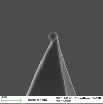
-Colloidal-
Various colloidal sphere-tips for direct surface force measurement, measurement of adhesion forces, studying of colloidal interactions between a particle and a surface and many other applications.
FMG01_BIO

Product Description
Special colloidal probes with spherical particles calibrated by size are fixed on the very end of the needle tip. SiO2 spheres are glued to High Resolution Silicon AFM Cantilevers FMG01 series specially designed for Force Modulation applications. Typical Resonant Frequency 60 kHz (guaranteed range 40-96kHz), Typical Force Constant 3 N/m (guaranteed range 1-5N/m). Cantilever has Au reflective side coating to increase laser signal. The possibility to operate in liquid with nanometer spatial resolution makes the AFM a unique instrument for the living cells studies. The accurate characterization of the mechanical properties of an individual cell is particularly actual, that can serve as an indicator of the important chemical and biological processes in the cell. The use of standard sharpened probes for the task is not always the best solution. A typical threshold for the local pressure that keeps the living cell intact may be just a few kPa. It is substantially lower than the pressure that locally acts on interacting of the sample with the standard probe. It can be reached with a so-called bioprobe with the smooth spherical colloidal particle of submicron size fi xed to the tip of the probe. If the size of the particle is calibrated, the opportunity to make quantitative researches of mechanical properties of the living cell, as well as of polymers is provided.
CSG30_BIO

Product Description
Special colloidal probes with spherical particles calibrated by size are fixed on the very end of the needle tip. SiO2 spheres are glued to High Resolution Silicon AFM Cantilevers CSG30 series which are designed for Contact/Noncontact applications. Typical Resonant Frequency 48 kHz (guaranteed range 26-76kHz), Typical Force Constant 0,6 N/m (guaranteed range 0,13-2N/m). Cantilever has Au reflective side coating to increase laser signal. The possibility to operate in liquid with nanometer spatial resolution makes the AFM a unique instrument for the living cells studies. The accurate characterization of the mechanical properties of an individual cell is particularly actual, that can serve as an indicator of the important chemical and biological processes in the cell. The use of standard sharpened probes for the task is not always the best solution. A typical threshold for the local pressure that keeps the living cell intact may be just a few kPa. It is substantially lower than the pressure that locally acts on interacting of the sample with the standard probe. It can be reached with a so-called bioprobe with the smooth spherical colloidal particle of submicron size fi xed to the tip of the probe. If the size of the particle is calibrated, the opportunity to make quantitative researches of mechanical properties of the living cell, as well as of polymers is provided.
NSG01_BIO
Product Description
Special colloidal probes with spherical particles calibrated by size are fixed on the very end of the needle tip. SiO2 spheres are glued to High Resolution Silicon AFM Cantilevers NSG01 series specially designed for Semicontact ( Intermittent ), Noncontact applications. Typical Resonant Frequency 150 kHz (guaranteed range 87-230kHz), Typical Force Constant 5.1 N/m (guaranteed range 1.45-15.1N/m). Cantilever has Au reflective side coating to increase laser signal. The possibility to operate in liquid with nanometer spatial resolution makes the AFM a unique instrument for the living cells studies. The accurate characterization of the mechanical properties of an individual cell is particularly actual, that can serve as an indicator of the important chemical and biological processes in the cell. The use of standard sharpened probes for the task is not always the best solution. A typical threshold for the local pressure that keeps the living cell intact may be just a few kPa. It is substantially lower than the pressure that locally acts on interacting of the sample with the standard probe. It can be reached with a so-called bioprobe with the smooth spherical colloidal particle of submicron size fi xed to the tip of the probe. If the size of the particle is calibrated, the opportunity to make quantitative researches of mechanical properties of the living cell, as well as of polymers is provided.
CPC
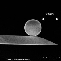
Product Description
Colloidal probes for Contact Mode with spherical particles calibrated by size fixed on the tipless cantilever. Sphere material SiO2/BSG, 4 sphere sizes from 5um till 20um, Au reflective coating, resonant frequency 8-37kHz, force constant 0,01-0,6N/m. Colloidal Probe Atomic Force Microscopy requires a tip of known shape to be mounted cleanly on a consistently reproducible cantilever. These probes are known as “Colloidal Probes” and are used to study colloidal interactions between two surfaces and to quantify the interactive properties. The tip is formed using a spherical, colloidal particle that is attached to a tipless cantilever. Сolloidal probes are manufactured in the state-of-the-art clean room using micromachining techniques and a high precision, 6 axis, micromanipulator stage system. Near perfect micro-spheres of various materials are attached at the end of tipless cantilevers using a proprietary, clean, contamination free process.
Colloidal Probe Application
Colloidal Probe applications include direct surface force measurement, colloidal interactions on the single particle-particle level, direct measurement of cell mechanics, measurement of adhesion forces, study of colloidal interactions between particle and surface. These are just a few application out of a fast growing field using colloidal probe technique.
-Single Crystal Diamond- 単結晶ダイヤモンドプローブ
The main probe advantages:
・High Resolution Diamond Tip – typical tip radius 7nm for both topography and electrical measurements.
・Endurance of Diamond - at least 10x Lifetime of Silicon.
・Standard AFM chip size.
Sharp, single crystal diamond AFM probes give the AFM user all the known resilience benefits of hard diamond, with no compromise on image resolution.
単結晶ダイヤモンドプローブ-DRP_In_C
Product Description
Calibrated Unique probes with Single Crystal Diamond tip specially designed for Nanoindentation, Nanoscratching, Lithography etc. Resonant frequency 500-1000kHz, force constant 100-600 N/m, curvature radius <15nm. These tips are specifically designed for high mechanical loads and scratch testing applications. By using wear-resistant diamond and a board cone angle the contact size is well characterized and stays constant during repeated mechanical measurements. These probes have demonstrated highly repeatable deep (~100nm) indentations into materials such as fused silica and are able to image the indents at high resolution in-situ using the same probe. A gold reflex coating deposited on the detector side of the cantilever to enhance the reflectance of the laser beam.
The probes are shipped with individually measured spring constant and a high resolution SEM image showing tip radius and cone angle. These probes are essentional for highly accurate nanoindentation and quantitative nanomechanics for materials in the 10-100 GPa range.
Nominal values: force constant - 350 N/m, resonance frequency – 750 kHz.
単結晶ダイヤモンドプローブ-DRP_In

Product Description
Unique probes with Single Crystal Diamond tip specially designed for Nanoindentation, Nanoscratching, Lithography etc. Resonant frequency 500-1000kHz, force constant 100-600 N/m, curvature radius <35nm. These tips are specifically designed for high mechanical loads and scratch testing applications. By using wear-resistant diamond and a board cone angle the contact size is well characterized and stays constant during repeated mechanical measurements. These probes have demonstrated highly repeatable deep (~100nm) indentations into materials such as fused silica and are able to image the indents at high resolution in-situ using the same probe. A gold reflex coating deposited on the detector side of the cantilever to enhance the reflectance of the laser beam.
The probes come with individual high resolution SEM image and ideally suited to scratch testing and long period probe lifetime applications where quantitative nanomechanics are not essential.
Nominal values: force constant - 350 N/m, resonance frequency – 750 kHz.
Upon customers' request the next options of single crystal probes are available:
- probes with individually characterized spring constant and tip radius to enable fully quantitative nanomechanical measurements.
単結晶ダイヤモンドプローブ-DRP30_SS
Product Description
Unique Super Sharp probes with single crystal diamond tip for topography measurements. The probes are highly resistant to mechanical destructions and keep their sharpness during the whole working day and more! These probes enable highly repeatable high resolution operation to ensure you consistently get the best possible data from your system. Nominal values: force constant - 40 N/m, resonance frequency – 180 kHz.
Upon customers' request the next options are available:
- super sharp probes with typical curvature radius 2nm;
- probes with another lever specification;
- probes with individually characterized spring constant and tip radius to enable fully quantitative nanomechanical measurements.
単結晶ダイヤモンドプローブ-DEP30
Product Description
Unique probes with single crystal diamond tip for topography and electrical measurements. Nominal values: force constant - 40 N/m, resonance frequency – 180 kHz. Highly Conductive Long Lasting Sharp Diamond Probes formed by a unique patented process ensure the best possible wear and electrical performance. The tips are sharper and last longer than any other electrical AFM probe. The probes are highly resistant to mechanical destructions and keep their sharpness during the whole working day and more! These probes enable highly repeatable high resolution operation to ensure you consistently get the best possible data from your system.
The conductive diamond coating is highly doped with boron which leads to a macroscopic resistivity of 0.003 - 0.005 Ohm•cm. A sharp tip is formed from a single diamond crystal which yields an unsurpassed combination of resolution, mechanical properties and electrical performance. Contact resistance is between 10k and 100k ohms depending on contact radius measured on a silver coated surface. A gold reflex coating is deposited on the detector side of the cantilever to enhance the reflectance of the laser beam.
Upon customers' request the next options are available:
- super sharp probes with typical curvature radius 2nm;
- probes with another lever specification;
- probes with individually characterized spring constant and tip radius to enable fully quantitative nanomechanical measurements.
単結晶ダイヤモンドプローブ-DEP01

Product Description
Unique probes with single crystal diamond tip for topography and electrical measurements. Nominal values: force constant - 2.8 N/m, resonance frequency – 75 kHz.
Highly Conductive Long Lasting Sharp Diamond Probes formed by a unique patented process ensure the best possible wear and electrical performance. The tips are sharper and last longer than any other electrical AFM probe.
The probes are highly resistant to mechanical destructions and keep their sharpness during the whole working day and more! These probes enable highly repeatable high resolution operation to ensure you consistently get the best possible data from your system.
The conductive diamond coating is highly doped with boron which leads to a macroscopic resistivity of 0.003 - 0.005 Ohm•cm. A sharp tip is formed from a single diamond crystal which yields an unsurpassed combination of resolution, mechanical properties and electrical performance. Contact resistance is between 10k and 100k ohms depending on contact radius measured on a silver coated surface. A gold reflex coating is deposited on the detector side of the cantilever to enhance the reflectance of the laser beam.
Upon customers' request the next options are available:
- super sharp probes with typical curvature radius 2nm;
- probes with another lever specification;
- probes with individually characterized spring constant and tip radius to enable fully quantitative nanomechanical measurements.
単結晶フルダイヤモンドプローブ-HA_NC/FD
Product Description
Long Lasting Probes with Single Crystal Full Diamond tip for noncontact/semicontact modes,
resonant frequency 140 kHz, force constant 3.5 N/m, typical curvature radius <10 nm.
走査型近接場光顕微鏡プローブ SNOM
SNOM — scanning near-field optical microscope, scanning near-field optical microscopy. In near-field optical microscopy uses different principles of construction of the image of object, which allow to overcome the difficulties associated with diffraction of light and to realize a spatial resolution of 10 nm and better. Higher resolution Bohm is achieved by detecting scattering of light from the object under study at distances smaller than the wavelength of light. In the case that the probe (detector) of the near-field microscope provided with a device for the spatial scan, the scanning device called optical near-field microscope. This microscope allows to obtain a raster image of surfaces and objects with a resolution below the diffraction limit.
-SNOM Cantilevers-
SNOM aperture cantilevers for Contact and Noncontact modes.
走査型近接場光顕微鏡プローブ SNOM_NC

Product Description
Set of 10 SNOM aperture cantilevers for NONCONTACT mode, resonance frequency 88-180 kHz, force constant 5.9-39 N/m.
Tip and lever specification
See corresponding pictures in the picture bar from the left.
・Tip shape - pyramidal
・Size of pyramid base, LxWxH = 20x20x13
・Pyramid angle - 70 degrees
・Pyramid material - SiO2
・Thickness of SiO2 - 400-600nm
・Tip coating - Al
・Thickness of Al coating ~ 100nm
・Aperture size - 150 ± 25nm
走査型近接場光顕微鏡プローブ SNOM_C
Product Description
Set of 10 SNOM aperture cantilevers for CONTACT mode, resonance frequency 15-27 kHz, force constant 0.4-2.3 N/m.
Tip and lever specification
See corresponding pictures in the picture bar from the left.
・Tip shape - pyramidal
・Size of pyramid base, LxWxH = 20x20x13
・Pyramid angle - 70 degrees
・Pyramid material - SiO2
・Thickness of SiO2 - 400-600nm
・Tip coating - Al
・Thickness of Al coating ~ 100nm
・Aperture size - 150 ± 25nm
-SNOM Fiber Probes- 走査型近接場光顕微鏡ファイバープローブ
SNOM PROBES - fiber probes with the formed aperture on the very tip end are specially designed for Scanning Near-Field Optical Microscopy. This method is used for investigating nanostructures at sub-wavelength scale.
Probes are produced from standard single-mode Nufern fibers by the method of chemical etching that provides better optical efficiency in comparison with mechanical pulling.
Probes perform all current modes of SNOM operation - transmission, reflection and collection.
We offer 5 types of transmitted wavelength:
・MF001 – 400-550 nm
・MF002 – 450-600 nm
・MF003 – 600-770 nm
・MF004 – 780-970 nm
・MF005 – 980-1600 nm
走査型近接場光顕微鏡ファイバープローブMF112_NTF

Product Description
SNOM fiber probes with glued quartz tuning-forks for NTEGRA line systems (NT-MDT Co.) with measuring head SNLG101NTF and Solver line systems with measuring head SNLG101.
Set of 10 SNOM probes with transmitted wavelength 450-600nm.
・Material - single mode optical fiber Nufern 460HP.
・Probe tip is coated by Al (70nm)/sublayer Cr (20nm) .
・Aperture (hole uncoated by Al) ~ 100 ± 30nm
・Angle of fiber - about 20 degrees
・Maximum optical input power - 400 microWatt
・Tip is formed by chemical etching.
・Fiber length ~ 2 meters.
・Tip length without protective coating is 7-8mm.
走査型近接場光顕微鏡ファイバープローブMF113_NTF

Product Description
SNOM fiber probes with glued quartz tuning-forks for NTEGRA line systems (NT-MDT Co.) with measuring head SNLG101NTF and Solver line systems with measuring head SNLG101.
Set of 10 SNOM probes with transmitted wavelength 600-770nm.
・Material - single mode optical fiber Nufern 630HP.
・Probe tip is coated by Al (70nm)/sublayer Cr (20nm) .
・Aperture (hole uncoated by Al) ~ 125±25 nm
・Angle of fiber - about 20 degrees
・Maximum optical input power - 400 microWatt
・Tip is formed by chemical etching.
・Fiber length ~ 2 meters.
・Tip length without protective coating is 7-8mm.
走査型近接場光顕微鏡ファイバープローブMF111_NTF
Product Description
SNOM fiber probes with glued quartz tuning-forks for NTEGRA line systems (NT-MDT Co.) with measuring head SNLG101NTF and Solver line systems with measuring head SNLG101. Set of 10 SNOM probes with transmitted wavelength 400-550nm.
・Material - single mode optical fiber Nufern 405HP.
・Probe tip is coated by Al (70nm)/sublayer Cr (20nm) .
・Aperture (hole uncoated by Al) ~ 50-100 nm
・Angle of fiber - about 20 degrees
・Maximum optical input power - 400 microWatt
・Tip is formed by chemical etching.
・Fiber length ~ 2 meters.
・Tip length without protective coating is 7-8mm.
走査型近接場光顕微鏡ファイバープローブMF114_NTF

Product Description
SNOM fiber probes with glued quartz tuning-forks for NTEGRA line systems (NT-MDT Co.) with measuring head SNLG101NTF and Solver line systems with measuring head SNLG101. Set of 10 SNOM probes with transmitted wavelength 780-970nm.
・Material - single mode optical fiber Nufern 780HP.
・Probe tip is coated by Al (70nm)/sublayer Cr (20nm) .
・Aperture (hole uncoated by Al) ~ 185±35 nm
・Angle of fiber - about 20 degrees
・Maximum optical input power - 400 microWatt
・Tip is formed by chemical etching.
・Fiber length ~ 2 meters.
・Tip length without protective coating is 7-8mm.
走査型近接場光顕微鏡ファイバープローブMF115_NTF

Product Description
SNOM fiber probes with glued quartz tuning-forks for NTEGRA line systems (NT-MDT Co.) with measuring head SNLG101NTF and Solver line systems with measuring head SNLG101. Set of 10 SNOM probes with transmitted wavelength 980-1600nm.
・Material - single mode optical fiber Nufern 980HP.
・Probe tip is coated by Al (70nm)/sublayer Cr (20nm) .
・Aperture (hole uncoated by Al) ~ 250 ± 50 nm
・Angle of fiber - about 20 degrees
・Maximum optical input power - 400 microWatt
・Tip is formed by chemical etching.
・Fiber length ~ 2 meters.
・Tip length without protective coating is 7-8mm.
走査型近接場光顕微鏡ファイバープローブMF001

Product Description
Set of 10 SNOM probes with transmitted wavelength 400-550nm.
・Material - single mode optical fiber Nufern 405HP.
・Probe tip is coated by Al (70nm)/sublayer Cr (20nm) .
・Aperture (hole uncoated by Al) ~ 50-100 nm
・Angle of fiber - about 20 degrees
・Maximum optical input power - 400 microWatt
・Tip is formed by chemical etching.
・Fiber length ~ 2 meters.
・Tip length without protective coating is 7-8mm.
走査型近接場光顕微鏡ファイバープローブMF002

Product Description
Set of 10 SNOM probes with transmitted wavelength 450-600nm.
・Material - single mode optical fiber Nufern 460HP.
・Probe tip is coated by Al (70nm)/sublayer Cr (20nm) .
・Aperture (hole uncoated by Al) ~ 100 ± 30 nm
・Angle of fiber - about 20 degrees
・Maximum optical input power - 400 microWatt
・Tip is formed by chemical etching.
・Fiber length ~ 2 meters.
・Tip length without protective coating is 7-8mm.
走査型近接場光顕微鏡ファイバープローブMF003

Product Description
Set of 10 SNOM probes with transmitted wavelength 600-770nm.
・Material - single mode optical fiber Nufern 630HP.
・Probe tip is coated by Al (70nm)/sublayer Cr (20nm) .
・Aperture (hole uncoated by Al) ~ 125 ± 25nm
・Angle of fiber - about 20 degrees
・Maximum optical input power - 400 microWatt
・Tip is formed by chemical etching.
・Fiber length ~ 2 meters.
・Tip length without protective coating is 7-8mm.
走査型近接場光顕微鏡ファイバープローブMF004

Product Description
Set of 10 SNOM probes with transmitted wavelength 780-970nm.
・Material - single mode optical fiber Nufern 780HP.
・Probe tip is coated by Al (70nm)/sublayer Cr (20nm) .
・Aperture (hole uncoated by Al) ~ 185 ± 35 nm.
・Angle of fiber - about 20 degrees
・Maximum optical input power - 400 microWatt
・Tip is formed by chemical etching.
・Fiber length ~ 2 meters.
・Tip length without protective coating is 7-8mm.
走査型近接場光顕微鏡ファイバープローブMF005
Product Description
Set of 10 SNOM probes with transmitted wavelength 980-1600nm.
・Material - single mode optical fiber Nufern 980HP.
・Probe tip is coated by Al (70nm)/sublayer Cr (20nm) .
・Aperture (hole uncoated by Al) ~ 250 ± 50 nm.
・Angle of fiber - about 20 degrees
・Maximum optical input power - 400 microWatt
・Tip is formed by chemical etching.
・Fiber length ~ 2 meters.
・Tip length without protective coating is 7-8mm.
TF001
Product Description
Set of 10 tuning forks for using in SNOM systems
TF101_NTF
Product Description
Set of 10 tuning forks for NTEGRA line systems with measuring head SNLG101NTF (NT-MDT Co) and Solver line systems with measuring head SNLG101.
-SNOM Test Grating-
SNG01
Product Description
Test grating for scanning near-field optical microscopy.
高配向性黒鉛基板HOPG
Highly Oriented Pyrolytic Graphite (HOPG). It’s a type of pure, highly laminar graphite used as an atomic-scale calibration standard for atomic force microscopy and scanning tunnelling microscopy. HOPG crystals are widely used as substrates in STM (Scanning Tunneling Microscopy). The most distinguishing features of HOPG which enable this application are a very smooth surface and electro conductivity. HOPG has a layered structure which makes sample preparation very simple. By pressing a double-stick tape to a HOPG piece and peeling it off, one gets a fresh conductive surface which is very smooth. This surface can be examined in STM or serve as a substrate for other materials under investigation. HOPG itself is an interesting object for STM investigations. One can measure the surface roughness, microscopic surface features, arrangement of the carbon atoms on the HOPG surface, etc. Besides, HOPG images at the atomic level can be used for calibrating STM for high-resolution imaging. 4 HOPG types (ZYA, ZYB, ZYD, ZYH) which differ by meaning of mosaic spread are available with sizes till 50x50mm. Both double-sided (DS) and single-sided (SS) HOPG pieces can be ordered. Double-sided HOPG can be used from both sides and its properties are not changed in depth. For one-sided piece the not working side is mat, glare less and can’t be cleaved. The number of working side cleavages of one-sided piece is limited in comparison with double sided substrate. The properties for one-sided piece are changed in depth.
-高配向性黒鉛基板(HOPG) ZYA quality-
HOPG of the highest quality. Mosaic Spread 0.4 ± 0.1 degrees. Available double- and single-sided. Double-sided HOPG can be used from both sides and its properties are not changed in depth. For one-sided piece the not working side is mat, glare less and can’t be cleaved. The number of working side cleavages of one-sided piece is limited in comparison with double sided substrate. The properties for one-sided piece are changed in depth.
高配向性黒鉛基板(HOPG) ZYA_DS, 10x10x2mm

Product Description
Highly Oriented Pyrolytic Graphite (HOPG) ZYA Quality, Mosaic Spread: 0.4 ± 0.1 degrees, double-sided, piece size – 10x10mm, thickness 2mm. Available size - till 50x50 mm. The best quality of the available HOPG types. Double-sided HOPG can be used from both sides and its properties are not changed in depth. For single-sided piece the not working side is mat, glare less and can’t be cleaved. The number of working side cleavages of one-sided piece is limited in comparison with double sided substrate. The properties for one-sided piece are changed in depth. HOPG crystals are widely used as substrates in STM (Scanning Tunneling Microscopy). The most distinguishing features of HOPG which enable this application are a very smooth surface and electro conductivity. HOPG has a layered structure which makes sample preparation very simple. By pressing a double-stick tape to a HOPG piece and peeling it off, one gets a fresh conductive surface which is very smooth. This surface can be examined in STM or serve as a substrate for other materials under investigation. HOPG itself is an interesting object for STM investigations. One can measure the surface roughness, microscopic surface features, arrangement of the carbon atoms on the HOPG surface, etc. Besides, HOPG images at the atomic level can be used for calibrating STM for high-resolution imaging.
高配向性黒鉛基板(HOPG) ZYA_DS, 12x12x2mm

Product Description
Highly Oriented Pyrolytic Graphite (HOPG) ZYA Quality, Mosaic Spread: 0.4 ± 0.1 degrees, double-sided, piece size – 12x12mm, thickness 2mm. Available size - till 50x50 mm. The best quality of the available HOPG types. Double-sided HOPG can be used from both sides and its properties are not changed in depth. For single-sided piece the not working side is mat, glare less and can’t be cleaved. The number of working side cleavages of one-sided piece is limited in comparison with double sided substrate. The properties for one-sided piece are changed in depth. HOPG crystals are widely used as substrates in STM (Scanning Tunneling Microscopy). The most distinguishing features of HOPG which enable this application are a very smooth surface and electro conductivity. HOPG has a layered structure which makes sample preparation very simple. By pressing a double-stick tape to a HOPG piece and peeling it off, one gets a fresh conductive surface which is very smooth. This surface can be examined in STM or serve as a substrate for other materials under investigation. HOPG itself is an interesting object for STM investigations. One can measure the surface roughness, microscopic surface features, arrangement of the carbon atoms on the HOPG surface, etc. Besides, HOPG images at the atomic level can be used for calibrating STM for high-resolution imaging.
高配向性黒鉛基板(HOPG) ZYA_DS, 10x10x1.5mm
Product Description
Highly Oriented Pyrolytic Graphite (HOPG) ZYA Quality, Mosaic Spread: 0.4 ± 0.1 degrees, double-sided, piece size – 10x10mm, thickness 1.5mm. Available size - till 50x50 mm. The best quality of the available HOPG types. Double-sided HOPG can be used from both sides and its properties are not changed in depth. For single-sided piece the not working side is mat, glare less and can’t be cleaved. The number of working side cleavages of one-sided piece is limited in comparison with double sided substrate. The properties for one-sided piece are changed in depth. HOPG crystals are widely used as substrates in STM (Scanning Tunneling Microscopy). The most distinguishing features of HOPG which enable this application are a very smooth surface and electro conductivity. HOPG has a layered structure which makes sample preparation very simple. By pressing a double-stick tape to a HOPG piece and peeling it off, one gets a fresh conductive surface which is very smooth. This surface can be examined in STM or serve as a substrate for other materials under investigation. HOPG itself is an interesting object for STM investigations. One can measure the surface roughness, microscopic surface features, arrangement of the carbon atoms on the HOPG surface, etc. Besides, HOPG images at the atomic level can be used for calibrating STM for high-resolution imaging.
高配向性黒鉛基板(HOPG) ZYA_DS, 12x12x1.5mm

Product Description
Highly Oriented Pyrolytic Graphite (HOPG) ZYA Quality, Mosaic Spread: 0.4 ± 0.1 degrees, double-sided, piece size – 12x12mm, thickness 1.5mm. Available size - till 50x50 mm. The best quality of the available HOPG types. Double-sided HOPG can be used from both sides and its properties are not changed in depth. For single-sided piece the not working side is mat, glare less and can’t be cleaved. The number of working side cleavages of one-sided piece is limited in comparison with double sided substrate. The properties for one-sided piece are changed in depth. HOPG crystals are widely used as substrates in STM (Scanning Tunneling Microscopy). The most distinguishing features of HOPG which enable this application are a very smooth surface and electro conductivity. HOPG has a layered structure which makes sample preparation very simple. By pressing a double-stick tape to a HOPG piece and peeling it off, one gets a fresh conductive surface which is very smooth. This surface can be examined in STM or serve as a substrate for other materials under investigation. HOPG itself is an interesting object for STM investigations. One can measure the surface roughness, microscopic surface features, arrangement of the carbon atoms on the HOPG surface, etc. Besides, HOPG images at the atomic level can be used for calibrating STM for high-resolution imaging.
高配向性黒鉛基板(HOPG) ZYA_DS, 10x10x1mm

Product Description
Highly Oriented Pyrolytic Graphite (HOPG) ZYA Quality, Mosaic Spread: 0.4 ± 0.1 degrees, double-sided, piece size – 10x10mm, thickness 1mm. Available size - till 50x50 mm. The best quality of the available HOPG types. Double-sided HOPG can be used from both sides and its properties are not changed in depth. For single-sided piece the not working side is mat, glare less and can’t be cleaved. The number of working side cleavages of one-sided piece is limited in comparison with double sided substrate. The properties for one-sided piece are changed in depth. HOPG crystals are widely used as substrates in STM (Scanning Tunneling Microscopy). The most distinguishing features of HOPG which enable this application are a very smooth surface and electro conductivity. HOPG has a layered structure which makes sample preparation very simple. By pressing a double-stick tape to a HOPG piece and peeling it off, one gets a fresh conductive surface which is very smooth. This surface can be examined in STM or serve as a substrate for other materials under investigation. HOPG itself is an interesting object for STM investigations. One can measure the surface roughness, microscopic surface features, arrangement of the carbon atoms on the HOPG surface, etc. Besides, HOPG images at the atomic level can be used for calibrating STM for high-resolution imaging.
高配向性黒鉛基板(HOPG) ZYA_DS, 12x12x1mm

Product Description
Highly Oriented Pyrolytic Graphite (HOPG) ZYA Quality, Mosaic Spread: 0.4 ± 0.1 degrees, double-sided, piece size – 12x12mm, thickness 1mm. Available size - till 50x50 mm. The best quality of the available HOPG types. Double-sided HOPG can be used from both sides and its properties are not changed in depth. For single-sided piece the not working side is mat, glare less and can’t be cleaved. The number of working side cleavages of one-sided piece is limited in comparison with double sided substrate. The properties for one-sided piece are changed in depth. HOPG crystals are widely used as substrates in STM (Scanning Tunneling Microscopy). The most distinguishing features of HOPG which enable this application are a very smooth surface and electro conductivity. HOPG has a layered structure which makes sample preparation very simple. By pressing a double-stick tape to a HOPG piece and peeling it off, one gets a fresh conductive surface which is very smooth. This surface can be examined in STM or serve as a substrate for other materials under investigation. HOPG itself is an interesting object for STM investigations. One can measure the surface roughness, microscopic surface features, arrangement of the carbon atoms on the HOPG surface, etc. Besides, HOPG images at the atomic level can be used for calibrating STM for high-resolution imaging.
-高配向性黒鉛基板(HOPG) ZYB quality-
Highly Oriented Pyrolytic Graphite (HOPG) ZYB quality. Mosaic Spread 0.8 ± 0.2 degrees. Available double- and single-sided. Double-sided HOPG can be used from both sides and its properties are not changed in depth. For one-sided piece the not working side is mat, glare less and can’t be cleaved. The number of working side cleavages of one-sided piece is limited in comparison with double sided substrate. The properties for one-sided piece are changed in depth.
高配向性黒鉛基板(HOPG) ZYB_DS, 10x10x2mm

Product Description
Highly Oriented Pyrolytic Graphite (HOPG) ZYB Quality, Mosaic Spread: 0.8 ± 0.2 degrees, double-sided, piece size – 10x10mm, thickness 2mm. Available size - till 50x50 mm. Double-sided HOPG can be used from both sides and its properties are not changed in depth. For single-sided piece the not working side is mat, glare less and can’t be cleaved. The number of working side cleavages of one-sided piece is limited in comparison with double sided substrate. The properties for one-sided piece are changed in depth. HOPG crystals are widely used as substrates in STM (Scanning Tunneling Microscopy). The most distinguishing features of HOPG which enable this application are a very smooth surface and electro conductivity. HOPG has a layered structure which makes sample preparation very simple. By pressing a double-stick tape to a HOPG piece and peeling it off, one gets a fresh conductive surface which is very smooth. This surface can be examined in STM or serve as a substrate for other materials under investigation. HOPG itself is an interesting object for STM investigations. One can measure the surface roughness, microscopic surface features, arrangement of the carbon atoms on the HOPG surface, etc. Besides, HOPG images at the atomic level can be used for calibrating STM for high-resolution imaging.
高配向性黒鉛基板(HOPG) ZYB_DS, 12x12x2mm
Product Description
Highly Oriented Pyrolytic Graphite (HOPG) ZYB Quality, Mosaic Spread: 0.8 ± 0.2 degrees, double-sided, piece size – 12x12mm, thickness 2mm. Available size - till 50x50 mm. Double-sided HOPG can be used from both sides and its properties are not changed in depth. For single-sided piece the not working side is mat, glare less and can’t be cleaved. The number of working side cleavages of one-sided piece is limited in comparison with double sided substrate. The properties for one-sided piece are changed in depth. HOPG crystals are widely used as substrates in STM (Scanning Tunneling Microscopy). The most distinguishing features of HOPG which enable this application are a very smooth surface and electro conductivity. HOPG has a layered structure which makes sample preparation very simple. By pressing a double-stick tape to a HOPG piece and peeling it off, one gets a fresh conductive surface which is very smooth. This surface can be examined in STM or serve as a substrate for other materials under investigation. HOPG itself is an interesting object for STM investigations. One can measure the surface roughness, microscopic surface features, arrangement of the carbon atoms on the HOPG surface, etc. Besides, HOPG images at the atomic level can be used for calibrating STM for high-resolution imaging.
高配向性黒鉛基板(HOPG) ZYB_DS, 10x10x1.5mm
Product Description
Highly Oriented Pyrolytic Graphite (HOPG) ZYB Quality, Mosaic Spread: 0.8 ± 0.2 degrees, double-sided, piece size – 10x10mm, thickness 1.5mm. Available size - till 50x50 mm. Double-sided HOPG can be used from both sides and its properties are not changed in depth. For single-sided piece the not working side is mat, glare less and can’t be cleaved. The number of working side cleavages of one-sided piece is limited in comparison with double sided substrate. The properties for one-sided piece are changed in depth. HOPG crystals are widely used as substrates in STM (Scanning Tunneling Microscopy). The most distinguishing features of HOPG which enable this application are a very smooth surface and electro conductivity. HOPG has a layered structure which makes sample preparation very simple. By pressing a double-stick tape to a HOPG piece and peeling it off, one gets a fresh conductive surface which is very smooth. This surface can be examined in STM or serve as a substrate for other materials under investigation. HOPG itself is an interesting object for STM investigations. One can measure the surface roughness, microscopic surface features, arrangement of the carbon atoms on the HOPG surface, etc. Besides, HOPG images at the atomic level can be used for calibrating STM for high-resolution imaging.
高配向性黒鉛基板(HOPG) ZYB_DS, 12x12x1.5mm
Product Description
Highly Oriented Pyrolytic Graphite (HOPG) ZYB Quality, Mosaic Spread: 0.8 ± 0.2 degrees, double-sided, piece size – 12x12mm, thickness 1.5mm. Available size - till 50x50 mm. Double-sided HOPG can be used from both sides and its properties are not changed in depth. For single-sided piece the not working side is mat, glare less and can’t be cleaved. The number of working side cleavages of one-sided piece is limited in comparison with double sided substrate. The properties for one-sided piece are changed in depth. HOPG crystals are widely used as substrates in STM (Scanning Tunneling Microscopy). The most distinguishing features of HOPG which enable this application are a very smooth surface and electro conductivity. HOPG has a layered structure which makes sample preparation very simple. By pressing a double-stick tape to a HOPG piece and peeling it off, one gets a fresh conductive surface which is very smooth. This surface can be examined in STM or serve as a substrate for other materials under investigation. HOPG itself is an interesting object for STM investigations. One can measure the surface roughness, microscopic surface features, arrangement of the carbon atoms on the HOPG surface, etc. Besides, HOPG images at the atomic level can be used for calibrating STM for high-resolution imaging.
高配向性黒鉛基板(HOPG) ZYB_DS, 10x10x1mm
Product Description
Highly Oriented Pyrolytic Graphite (HOPG) ZYB Quality, Mosaic Spread: 0.8 ± 0.2 degrees, double-sided, piece size – 10x10mm, thickness 1mm. Available size - till 50x50 mm. Double-sided HOPG can be used from both sides and its properties are not changed in depth. For single-sided piece the not working side is mat, glare less and can’t be cleaved. The number of working side cleavages of one-sided piece is limited in comparison with double sided substrate. The properties for one-sided piece are changed in depth. HOPG crystals are widely used as substrates in STM (Scanning Tunneling Microscopy). The most distinguishing features of HOPG which enable this application are a very smooth surface and electro conductivity. HOPG has a layered structure which makes sample preparation very simple. By pressing a double-stick tape to a HOPG piece and peeling it off, one gets a fresh conductive surface which is very smooth. This surface can be examined in STM or serve as a substrate for other materials under investigation. HOPG itself is an interesting object for STM investigations. One can measure the surface roughness, microscopic surface features, arrangement of the carbon atoms on the HOPG surface, etc. Besides, HOPG images at the atomic level can be used for calibrating STM for high-resolution imaging.
高配向性黒鉛基板(HOPG) ZYB_DS, 12x12x1mm
Product Description
Highly Oriented Pyrolytic Graphite (HOPG) ZYB Quality, Mosaic Spread: 0.8 ± 0.2 degrees, single-sided, piece size – 10x10mm, thickness 2mm. Available size - till 50x50 mm. Double-sided HOPG can be used from both sides and its properties are not changed in depth. For single-sided piece the not working side is mat, glare less and can’t be cleaved. The number of working side cleavages of one-sided piece is limited in comparison with double sided substrate. The properties for one-sided piece are changed in depth. HOPG crystals are widely used as substrates in STM (Scanning Tunneling Microscopy). The most distinguishing features of HOPG which enable this application are a very smooth surface and electro conductivity. HOPG has a layered structure which makes sample preparation very simple. By pressing a double-stick tape to a HOPG piece and peeling it off, one gets a fresh conductive surface which is very smooth. This surface can be examined in STM or serve as a substrate for other materials under investigation. HOPG itself is an interesting object for STM investigations. One can measure the surface roughness, microscopic surface features, arrangement of the carbon atoms on the HOPG surface, etc. Besides, HOPG images at the atomic level can be used for calibrating STM for high-resolution imaging.
高配向性黒鉛基板(HOPG) ZYB_DS, 10x10x1.5mm
Product Description
Highly Oriented Pyrolytic Graphite (HOPG) ZYB Quality, Mosaic Spread: 0.8 ± 0.2 degrees, single-sided, piece size – 10x10mm, thickness 1.5mm. Available size - till 50x50 mm. Double-sided HOPG can be used from both sides and its properties are not changed in depth. For single-sided piece the not working side is mat, glare less and can’t be cleaved. The number of working side cleavages of one-sided piece is limited in comparison with double sided substrate. The properties for one-sided piece are changed in depth. HOPG crystals are widely used as substrates in STM (Scanning Tunneling Microscopy). The most distinguishing features of HOPG which enable this application are a very smooth surface and electro conductivity. HOPG has a layered structure which makes sample preparation very simple. By pressing a double-stick tape to a HOPG piece and peeling it off, one gets a fresh conductive surface which is very smooth. This surface can be examined in STM or serve as a substrate for other materials under investigation. HOPG itself is an interesting object for STM investigations. One can measure the surface roughness, microscopic surface features, arrangement of the carbon atoms on the HOPG surface, etc. Besides, HOPG images at the atomic level can be used for calibrating STM for high-resolution imaging.
高配向性黒鉛基板(HOPG) ZYB_DS, 10x10x1mm
Product Description
Highly Oriented Pyrolytic Graphite (HOPG) ZYB Quality, Mosaic Spread: 0.8 ± 0.2 degrees, single-sided, piece size – 10x10mm, thickness 1mm. Available size - till 50x50 mm. Double-sided HOPG can be used from both sides and its properties are not changed in depth. For single-sided piece the not working side is mat, glare less and can’t be cleaved. The number of working side cleavages of one-sided piece is limited in comparison with double sided substrate. The properties for one-sided piece are changed in depth. HOPG crystals are widely used as substrates in STM (Scanning Tunneling Microscopy). The most distinguishing features of HOPG which enable this application are a very smooth surface and electro conductivity. HOPG has a layered structure which makes sample preparation very simple. By pressing a double-stick tape to a HOPG piece and peeling it off, one gets a fresh conductive surface which is very smooth. This surface can be examined in STM or serve as a substrate for other materials under investigation. HOPG itself is an interesting object for STM investigations. One can measure the surface roughness, microscopic surface features, arrangement of the carbon atoms on the HOPG surface, etc. Besides, HOPG images at the atomic level can be used for calibrating STM for high-resolution imaging.
-高配向性黒鉛基板(HOPG) ZYD quality-
Highly Oriented Pyrolytic Graphite (HOPG) ZYD quality. Mosaic Spread 1.7 ± 0.4 degrees. Available double- and single-sided. Double-sided HOPG can be used from both sides and its properties are not changed in depth. For one-sided piece the not working side is mat, glare less and can’t be cleaved. The number of working side cleavages of one-sided piece is limited in comparison with double sided substrate. The properties for one-sided piece are changed in depth.
高配向性黒鉛基板(HOPG) ZYD_DS, 10x10x2mm
Product Description
Highly Oriented Pyrolytic Graphite (HOPG) ZYD Quality, Mosaic Spread: 1.7 ± 0.4 degrees, double-sided, piece size – 10x10mm, thickness 2mm. Available size - till 50x50 mm.
Double-sided HOPG can be used from both sides and its properties are not changed in depth.
For single-sided piece the not working side is mat, glare less and can’t be cleaved. The number of working side cleavages of one-sided piece is limited in comparison with double sided substrate. The properties for one-sided piece are changed in depth.
HOPG crystals are widely used as substrates in STM (Scanning Tunneling Microscopy). The most distinguishing features of HOPG which enable this application are a very smooth surface and electro conductivity.
HOPG has a layered structure which makes sample preparation very simple. By pressing a double-stick tape to a HOPG piece and peeling it off, one gets a fresh conductive surface which is very smooth. This surface can be examined in STM or serve as a substrate for other materials under investigation.
HOPG itself is an interesting object for STM investigations. One can measure the surface roughness, microscopic surface features, arrangement of the carbon atoms on the HOPG surface, etc. Besides, HOPG images at the atomic level can be used for calibrating STM for high-resolution imaging.
高配向性黒鉛基板(HOPG) ZYD_DS, 12x12x2mm
Product Description
Highly Oriented Pyrolytic Graphite (HOPG) ZYD Quality, Mosaic Spread: 1.7 ± 0.4 degrees, double-sided, piece size – 12x12mm, thickness 2mm. Available size - till 50x50 mm.
Double-sided HOPG can be used from both sides and its properties are not changed in depth.
For single-sided piece the not working side is mat, glare less and can’t be cleaved. The number of working side cleavages of one-sided piece is limited in comparison with double sided substrate. The properties for one-sided piece are changed in depth.
HOPG crystals are widely used as substrates in STM (Scanning Tunneling Microscopy). The most distinguishing features of HOPG which enable this application are a very smooth surface and electro conductivity.
HOPG has a layered structure which makes sample preparation very simple. By pressing a double-stick tape to a HOPG piece and peeling it off, one gets a fresh conductive surface which is very smooth. This surface can be examined in STM or serve as a substrate for other materials under investigation.
HOPG itself is an interesting object for STM investigations. One can measure the surface roughness, microscopic surface features, arrangement of the carbon atoms on the HOPG surface, etc. Besides, HOPG images at the atomic level can be used for calibrating STM for high-resolution imaging.
高配向性黒鉛基板(HOPG) ZYD_DS, 10x10x1.5mm
Product Description
Highly Oriented Pyrolytic Graphite (HOPG) ZYD Quality, Mosaic Spread: 1.7 ± 0.4 degrees, double-sided, piece size – 12x12mm, thickness 1.5 mm. Available size - till 50x50 mm.
Double-sided HOPG can be used from both sides and its properties are not changed in depth.
For single-sided piece the not working side is mat, glare less and can’t be cleaved. The number of working side cleavages of one-sided piece is limited in comparison with double sided substrate. The properties for one-sided piece are changed in depth.
HOPG crystals are widely used as substrates in STM (Scanning Tunneling Microscopy). The most distinguishing features of HOPG which enable this application are a very smooth surface and electro conductivity.
HOPG has a layered structure which makes sample preparation very simple. By pressing a double-stick tape to a HOPG piece and peeling it off, one gets a fresh conductive surface which is very smooth. This surface can be examined in STM or serve as a substrate for other materials under investigation.
HOPG itself is an interesting object for STM investigations. One can measure the surface roughness, microscopic surface features, arrangement of the carbon atoms on the HOPG surface, etc. Besides, HOPG images at the atomic level can be used for calibrating STM for high-resolution imaging.
高配向性黒鉛基板(HOPG) ZYD_DS, 10x10x1mm
Product Description
Highly Oriented Pyrolytic Graphite (HOPG) ZYD Quality, Mosaic Spread: 1.7 ± 0.4 degrees, double-sided, piece size – 10x10mm, thickness 1.0 mm. Available size - till 50x50 mm.
Double-sided HOPG can be used from both sides and its properties are not changed in depth.
For single-sided piece the not working side is mat, glare less and can’t be cleaved. The number of working side cleavages of one-sided piece is limited in comparison with double sided substrate. The properties for one-sided piece are changed in depth.
HOPG crystals are widely used as substrates in STM (Scanning Tunneling Microscopy). The most distinguishing features of HOPG which enable this application are a very smooth surface and electro conductivity.
HOPG has a layered structure which makes sample preparation very simple. By pressing a double-stick tape to a HOPG piece and peeling it off, one gets a fresh conductive surface which is very smooth. This surface can be examined in STM or serve as a substrate for other materials under investigation.
HOPG itself is an interesting object for STM investigations. One can measure the surface roughness, microscopic surface features, arrangement of the carbon atoms on the HOPG surface, etc. Besides, HOPG images at the atomic level can be used for calibrating STM for high-resolution imaging.
高配向性黒鉛基板(HOPG) ZYD_DS, 12x12x1mm
Product Description
Highly Oriented Pyrolytic Graphite (HOPG) ZYD Quality, Mosaic Spread: 1.7 ± 0.4 degrees, double-sided, piece size – 12x12mm, thickness 1.0 mm. Available size - till 50x50 mm.
Double-sided HOPG can be used from both sides and its properties are not changed in depth.
For single-sided piece the not working side is mat, glare less and can’t be cleaved. The number of working side cleavages of one-sided piece is limited in comparison with double sided substrate. The properties for one-sided piece are changed in depth.
HOPG crystals are widely used as substrates in STM (Scanning Tunneling Microscopy). The most distinguishing features of HOPG which enable this application are a very smooth surface and electro conductivity.
HOPG has a layered structure which makes sample preparation very simple. By pressing a double-stick tape to a HOPG piece and peeling it off, one gets a fresh conductive surface which is very smooth. This surface can be examined in STM or serve as a substrate for other materials under investigation.
HOPG itself is an interesting object for STM investigations. One can measure the surface roughness, microscopic surface features, arrangement of the carbon atoms on the HOPG surface, etc. Besides, HOPG images at the atomic level can be used for calibrating STM for high-resolution imaging.
高配向性黒鉛基板(HOPG) ZYD_SS, 10x10x2mm
Product Description
Highly Oriented Pyrolytic Graphite (HOPG) ZYD Quality, Mosaic Spread: 1.7 ± 0.4 degrees, single-sided, piece size – 10x10mm, thickness 2mm. Available size - till 50x50 mm.
Double-sided HOPG can be used from both sides and its properties are not changed in depth.
For single-sided piece the not working side is mat, glare less and can’t be cleaved. The number of working side cleavages of one-sided piece is limited in comparison with double sided substrate. The properties for one-sided piece are changed in depth.
HOPG crystals are widely used as substrates in STM (Scanning Tunneling Microscopy). The most distinguishing features of HOPG which enable this application are a very smooth surface and electro conductivity.
HOPG has a layered structure which makes sample preparation very simple. By pressing a double-stick tape to a HOPG piece and peeling it off, one gets a fresh conductive surface which is very smooth. This surface can be examined in STM or serve as a substrate for other materials under investigation.
HOPG itself is an interesting object for STM investigations. One can measure the surface roughness, microscopic surface features, arrangement of the carbon atoms on the HOPG surface, etc. Besides, HOPG images at the atomic level can be used for calibrating STM for high-resolution imaging.
高配向性黒鉛基板(HOPG) ZYD_SS, 10x10x1.5mm
Product Description
Highly Oriented Pyrolytic Graphite (HOPG) ZYD Quality, Mosaic Spread: 1.7 ± 0.4 degrees, single-sided, piece size – 10x10mm, thickness 1.5 mm. Available size - till 50x50 mm.
Double-sided HOPG can be used from both sides and its properties are not changed in depth. For single-sided piece the not working side is mat, glare less and can’t be cleaved. The number of working side cleavages of one-sided piece is limited in comparison with double sided substrate. The properties for one-sided piece are changed in depth.
HOPG crystals are widely used as substrates in STM (Scanning Tunneling Microscopy). The most distinguishing features of HOPG which enable this application are a very smooth surface and electro conductivity.
HOPG has a layered structure which makes sample preparation very simple. By pressing a double-stick tape to a HOPG piece and peeling it off, one gets a fresh conductive surface which is very smooth. This surface can be examined in STM or serve as a substrate for other materials under investigation.
HOPG itself is an interesting object for STM investigations. One can measure the surface roughness, microscopic surface features, arrangement of the carbon atoms on the HOPG surface, etc. Besides, HOPG images at the atomic level can be used for calibrating STM for high-resolution imaging.
高配向性黒鉛基板(HOPG) ZYD_SS, 10x10x1mm
Product Description
Highly Oriented Pyrolytic Graphite (HOPG) ZYD Quality, Mosaic Spread: 1.7 ± 0.4 degrees, single-sided, piece size – 10x10mm, thickness 1.0 mm. Available size - till 50x50 mm.
Double-sided HOPG can be used from both sides and its properties are not changed in depth.
For single-sided piece the not working side is mat, glare less and can’t be cleaved. The number of working side cleavages of one-sided piece is limited in comparison with double sided substrate. The properties for one-sided piece are changed in depth. HOPG crystals are widely used as substrates in STM (Scanning Tunneling Microscopy). The most distinguishing features of HOPG which enable this application are a very smooth surface and electro conductivity.
HOPG has a layered structure which makes sample preparation very simple. By pressing a double-stick tape to a HOPG piece and peeling it off, one gets a fresh conductive surface which is very smooth. This surface can be examined in STM or serve as a substrate for other materials under investigation.
HOPG itself is an interesting object for STM investigations. One can measure the surface roughness, microscopic surface features, arrangement of the carbon atoms on the HOPG surface, etc. Besides, HOPG images at the atomic level can be used for calibrating STM for high-resolution imaging.
-高配向性黒鉛基板(HOPG) ZYH quality-
Highly Oriented Pyrolytic Graphite (HOPG) ZYH quality. Mosaic Spread 3.5 ± 1.5 degrees. Available only double-sided. Double-sided HOPG can be used from both sides and its properties are not changed in depth.
高配向性黒鉛基板(HOPG) ZYH_DS, 10x10x2mm
Product Description
Highly Oriented Pyrolytic Graphite (HOPG) ZYH Quality, Mosaic Spread: 3.5 ± 1.5 degrees, double-sided, piece size – 10x10mm, thickness 2mm. Available size - till 50x50 mm.
Double-sided HOPG can be used from both sides and its properties are not changed in depth.
HOPG crystals are widely used as substrates in STM (Scanning Tunneling Microscopy). The most distinguishing features of HOPG which enable this application are a very smooth surface and electro conductivity.
HOPG has a layered structure which makes sample preparation very simple. By pressing a double-stick tape to a HOPG piece and peeling it off, one gets a fresh conductive surface which is very smooth. This surface can be examined in STM or serve as a substrate for other materials under investigation.
HOPG itself is an interesting object for STM investigations. One can measure the surface roughness, microscopic surface features, arrangement of the carbon atoms on the HOPG surface, etc. Besides, HOPG images at the atomic level can be used for calibrating STM for high-resolution imaging.
高配向性黒鉛基板(HOPG) ZYH_DS, 12x12x2mm
Product Description
Highly Oriented Pyrolytic Graphite (HOPG) ZYH Quality, Mosaic Spread: 3.5 ± 1.5 degrees, double-sided, piece size – 12x12mm, thickness 2mm. Available size - till 50x50 mm.
Double-sided HOPG can be used from both sides and its properties are not changed in depth.
HOPG crystals are widely used as substrates in STM (Scanning Tunneling Microscopy). The most distinguishing features of HOPG which enable this application are a very smooth surface and electro conductivity.
HOPG has a layered structure which makes sample preparation very simple. By pressing a double-stick tape to a HOPG piece and peeling it off, one gets a fresh conductive surface which is very smooth. This surface can be examined in STM or serve as a substrate for other materials under investigation.
HOPG itself is an interesting object for STM investigations. One can measure the surface roughness, microscopic surface features, arrangement of the carbon atoms on the HOPG surface, etc. Besides, HOPG images at the atomic level can be used for calibrating STM for high-resolution imaging.
高配向性黒鉛基板(HOPG) ZYH_DS, 10x10x1.5mm
Product Description
Highly Oriented Pyrolytic Graphite (HOPG) ZYH Quality, Mosaic Spread: 3.5 ± 1.5 degrees, double-sided, piece size – 10x10mm, thickness 1.5 mm. Available size - till 50x50 mm.
Double-sided HOPG can be used from both sides and its properties are not changed in depth.
HOPG crystals are widely used as substrates in STM (Scanning Tunneling Microscopy). The most distinguishing features of HOPG which enable this application are a very smooth surface and electro conductivity.
HOPG has a layered structure which makes sample preparation very simple. By pressing a double-stick tape to a HOPG piece and peeling it off, one gets a fresh conductive surface which is very smooth. This surface can be examined in STM or serve as a substrate for other materials under investigation.
HOPG itself is an interesting object for STM investigations. One can measure the surface roughness, microscopic surface features, arrangement of the carbon atoms on the HOPG surface, etc. Besides, HOPG images at the atomic level can be used for calibrating STM for high-resolution imaging.
高配向性黒鉛基板(HOPG) ZYH_DS, 12x12x1.5mm
Product Description
Highly Oriented Pyrolytic Graphite (HOPG) ZYH Quality, Mosaic Spread: 3.5 ± 1.5 degrees, double-sided, piece size – 12x12mm, thickness 1.5 mm. Available size - till 50x50 mm.
Double-sided HOPG can be used from both sides and its properties are not changed in depth.
HOPG crystals are widely used as substrates in STM (Scanning Tunneling Microscopy). The most distinguishing features of HOPG which enable this application are a very smooth surface and electro conductivity.
HOPG has a layered structure which makes sample preparation very simple. By pressing a double-stick tape to a HOPG piece and peeling it off, one gets a fresh conductive surface which is very smooth. This surface can be examined in STM or serve as a substrate for other materials under investigation.
HOPG itself is an interesting object for STM investigations. One can measure the surface roughness, microscopic surface features, arrangement of the carbon atoms on the HOPG surface, etc. Besides, HOPG images at the atomic level can be used for calibrating STM for high-resolution imaging.
高配向性黒鉛基板(HOPG) ZYH_DS, 10x10x1mm
Product Description
Highly Oriented Pyrolytic Graphite (HOPG) ZYH Quality, Mosaic Spread: 3.5 ± 1.5 degrees, double-sided, piece size – 10x10mm, thickness 1.0 mm. Available size - till 50x50 mm.
Double-sided HOPG can be used from both sides and its properties are not changed in depth.
HOPG crystals are widely used as substrates in STM (Scanning Tunneling Microscopy). The most distinguishing features of HOPG which enable this application are a very smooth surface and electro conductivity.
HOPG has a layered structure which makes sample preparation very simple. By pressing a double-stick tape to a HOPG piece and peeling it off, one gets a fresh conductive surface which is very smooth. This surface can be examined in STM or serve as a substrate for other materials under investigation.
HOPG itself is an interesting object for STM investigations. One can measure the surface roughness, microscopic surface features, arrangement of the carbon atoms on the HOPG surface, etc. Besides, HOPG images at the atomic level can be used for calibrating STM for high-resolution imaging.
高配向性黒鉛基板(HOPG) ZYH_DS, 12x12x1mm
Product Description
Highly Oriented Pyrolytic Graphite (HOPG) ZYH Quality, Mosaic Spread: 3.5 ± 1.5 degrees, double-sided, piece size – 12x12mm, thickness 1.0 mm. Available size - till 50x50 mm.
Double-sided HOPG can be used from both sides and its properties are not changed in depth.
HOPG crystals are widely used as substrates in STM (Scanning Tunneling Microscopy). The most distinguishing features of HOPG which enable this application are a very smooth surface and electro conductivity.
HOPG has a layered structure which makes sample preparation very simple. By pressing a double-stick tape to a HOPG piece and peeling it off, one gets a fresh conductive surface which is very smooth. This surface can be examined in STM or serve as a substrate for other materials under investigation.
HOPG itself is an interesting object for STM investigations. One can measure the surface roughness, microscopic surface features, arrangement of the carbon atoms on the HOPG surface, etc. Besides, HOPG images at the atomic level can be used for calibrating STM for high-resolution imaging.
Calibration AFM校正試験用サンプル
To determine the credibility of studies by AFM — microscopy testing and calibration of microscope work and test the quality of probes (scale of X-, Y-, Z - coordinates, the radius of the tip of the cantilever, linearity and orthogonality of the axes of the scan). For calibration and determination of the working shapes of the probes used special test structures with known topography.
For the calibration of microscopes in the scanning plane and vertically apply a diffraction grating with submicron sizes. In the absence of a specially manufactured calibration gratings, can be used as a test object to obtain atomic resolution fresh cleaved mica or highly oriented pyrolytic graphite (HOPG), because the parameters of the terrain are well known.
Advantages of graphite as the test sample are: stable operation is output; a low concentration of point and line defects; low reactivity in atmospheric conditions; the possibility of obtaining atomically clean surface.
-Calibration Gratings-
The full set of calibration standards for AFM lateral and vertical calibration including submicron calibration in X or/and Y direction, test grating for the tip shape estimation, Highly Oriented Pyrolytic Graphite (HOPG), DNA and PFM test samples.
TGG1
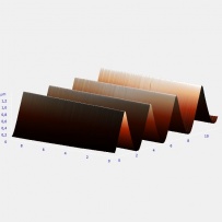
Product Description
Calibration grating TGG1 is intended for
・AFM calibration in X or Y axis;
・detection of lateral and vertical scanner nonlinearity;
・detection of angular distortion;
・tip characterization.
TGZ1
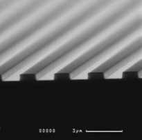
Product Description
Calibration grating TGZ1 for Z-axis calibration (step height 20,0±1.5nm) and nonlinearity measurements.
Step height is the average meaning based on the measurements of 5 gratings with the same height (from the batch of 300 gratings) by AFM calibrated wih help of PTB certified grating TGZ1. Basic step height can vary from the specified one within ±10 % depending on the batch (for example TGZ1 grating can have step height 22±1.5 nm).
TGZ2

Product Description
Calibration grating TGZ2 is intended for Z-axis calibration (step height 110 ± 2 nm) and nonlinearity measurements.
Step height is the average meaning based on the measurements of 5 gratings with the same height (from the batch of 300 gratings) by AFM calibrated wih help of PTB certified grating TGZ1. Basic step height can vary from the specified one within ±20 % depending on the batch (for example TGZ2 grating can have step height 95±2 nm).
TGQ1

Product Description
Calibration grating TGQ1 is intended for
・simultaneous calibration in X, Y and Z directions;
・scanner lateral calibration;
・detection of lateral non-linearity, hysteresis, creep and cross-coupling effects.
Step height is the average meaning based on the measurements of 5 gratings with the same height (from the batch of 300 gratings) by AFM calibrated wih help of PTB certified grating TGZ1. Basic step height can vary from the specified one within ±15% depending on the batch (for example step height can be 23±1.5 nm).
TGT1
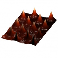
Product Description
Calibration grating TGT1 is intended for
・tip shape and sharpness estimation and further using in deconvolution program;
・tip degradation and contamination control.
TGZ3

Product Description
Calibration grating TGZ3 for Z-axis calibration (step height 520 ± 3 nm) and nonlinearity measurements.
Step height is the average meaning based on the measurements of 5 gratings with the same height (from the batch of 300 gratings) by AFM calibrated wih help of PTB certified grating TGZ3. Basic step height can vary from the specified one within ±15 % depending on the batch (for example TGZ3 grating can have step height 580±3 nm).
TGZ4

Product Description
Calibration grating TGZ4 for Z-axis calibration (step height 1517±20nm) and nonlinearity measurements.
Step height is the average meaning based on the measurements of 5 gratings with the same height (from the batch of 300 gratings) by AFM calibrated wih help of PTB certified grating TGZ1. Basic step height can vary from the specified one within ±10 % depending on the batch (for example TGZ4 grating can have step height 1600±20 nm).
TGX1
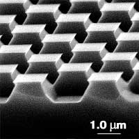
Product Description
Calibration grating TGX1 is intended for
・lateral calibration of AFM scanners
・detection of lateral non-linearity, hysteresis, creep, and cross-coupling effects;
・determination of the tip sharpness.
TDG01
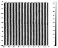
Product Description
Calibration grating TDG01 is intended for AFM submicron calibration in X or Y direction. Period is 278nm.
-Grating sets-
Grating sets at optimal cost for AFM calibrationg and tip characterization.
TGS1F

Product Description
Grating set TGS1 consists of 4 calibration gratings: TGZ1, TGZ2, TGZ3, TGZ4 and intended for Z and X (or Y) calibration and nonlinearity measurements.
TGSFull

Product Description
Grating set TGSFull consists of 8 calibration gratings: TGZ1, TGZ2, TGZ3, TGT1, TGQ1, TGG1, TGX1, TDG01.
Grating set TGSFull can be used for:
・SPM simultaneuos calibration in X, Y and Z directions;
・submicron SPM calibration in X or Y direction;
・lateral and vertical calibration;
・detection of lateral non-linearity;
・detection of hysteresis, creep, and cross-coupling effects;
・detection of angular distortion;
・for 3-D visualization of the scanning tip;
・determination of tip sharpness parameters (aspect ratio and curvature radius), tip degradation and contamination control.
TGS1_PTB
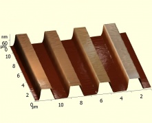
Product Description
Grating set TGS1 (consists of three gratings TGZ1, TGZ2, TGZ3) can be ordered with PTB traceable certificate. The gratings TGS1_PTB are measured on the AFM which has been preliminary calibrated using the PTB certified grating set TGS1. Step heights: 20±1.5nm, 110±2nm, 520±3nm. In comparision with TGS1 grating set you will have height meanings with lower uncertainties that will help to obtained more reliable scans of the scanned objects.
TGS2
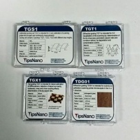
Product Description
Grating set TGS2 consists of 6 calibration gratings: TGZ1, TGZ2, TGZ3, TGT1, TGG1, TGX1.
Grating set TGS2 can be used for:
・AFM calibration in X, Y and Z directions;
・lateral and vertical calibration;
・detection of lateral non-linearity;
・detection of hysteresis, creep, and cross-coupling effects;
・detection of angular distortion;
・for 3-D visualization of the scanning tip;
・determination of tip sharpness parameters (aspect ratio and curvature radius), tip degradation and contamination control.
TGS1
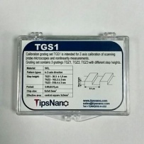
Product Description
Grating set TGS1 consists of 3 calibration gratings: TGZ1, TGZ2, TGZ3 nad intended for Z and X (or Y) calibration and nonlinearity measurements.
TGS_Cert
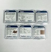
Product Description
Grating set TGS_Cert consists of 7 calibration gratings: TGZ1, TGZ2, TGZ3, TGT1, TGQ1, TGG1, TDG01.
Grating set TGS_Cert can be used for:
・SPM simultaneuos calibration in X, Y and Z directions;
・submicron SPM calibration in X or Y direction;
・lateral and vertical calibration;
・detection of lateral non-linearity;
・detection of hysteresis, creep, and cross-coupling effects;
・detection of angular distortion;
・for 3-D visualization of the scanning tip;
・determination of tip sharpness parameters (aspect ratio and curvature radius), tip degradation and contamination control.
-Substrates-
雲母基板・マイカ・Mica/15x15
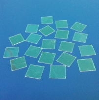
Product Description
Square mica, 0.15 mm (0.006") thickness, size 15 mm x 15 mm.
Specification:
Specific Gravity (water = 1.0): 2.7
Chemical Formula: K2O·Al2O3·SiO2
Hardness on Mohs scale of hardness: 2 - 2.25
Thickness = 0.15 mm (0.006")
Lateral Size = 15 x 15 mm
SU001
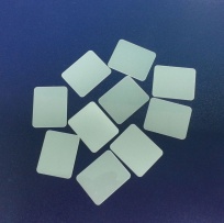
Product Description
Set of 10 substrates of polycrystalline sapphire.
Size 24x19,3x0,5mm.
雲母基板・マイカ・Mica/d9.5
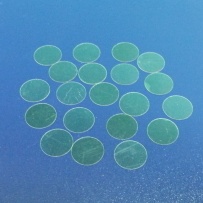
Product Description
Mica Disks, 0.15 mm (0.006") thickness, size 9.5 mm diameter.
Specification:
Specific Gravity (water = 1.0): 2.7
Chemical Formula: K2O·Al2O3·SiO2
Hardness on Mohs scale of hardness: 2 - 2.25
Thickness = 0.15 mm (0.006")
Diameter = 9.5 mm diameter
-Test Samples-
DNA01
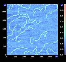
Product Description
DNA01 is Plasmid pGem7zf+ (Promega) which is linearized with the SmaI endonuclease. A linear DNA molecules (3000 b. p.) are deposited onto freshly cleaved mica. Molecules are uniformly distributed on the surface with molecule density - 0,5-7 molec./um2 and typical DNA length 1009nm. Recommended humidity for obtaining a good image is 3-5%.
Applications:
- getting start in working on AFM with biological samples;
- using like a sample for preparing DNA samples by your own;
- estimation of cantilevers tip radius curvature (since the DNA size is equal two nanometres in free condition);
- test samples for Z-resolution of commercial SPMs.
SiC/0.75

Product Description
6H-SiC(0001) based calibration sample is designed to perform easy calibrations of AFM scanner vertical movement in subnanometer intervals. The simplicity of calibration process is provided by nearly uniform distribution of half-monolayer high (0.75 nm) steps on the sample surface demonstrating chemical and mechanical stability. The step height corresponds to the half of lattice constant of 6H-SiC crystal in [0001] direction.
Specification:
・Chip size – 5x5x0.3 mm3
・Average interstep distance – 0.15-0.4 µm
・Misorientation of surface ~ 0.2°
・Single step height 0.75 nm
・Average roughness of the area between steps (terraces) – 0.09 nm
SiC/1.5
Product Description
6H-SiC(0001) based calibration sample is designed to perform easy calibrations of AFM scanner vertical movement in several nanometer intervals. The simplicity of calibration process is provided by nearly uniform distribution of monolayer high (1.5 nm) steps on the sample surface demonstrating chemical and mechanical stability. The step height corresponds to the lattice constant of 6H-SiC crystal in [0001] direction.
Specification:
・Chip size – 5x5x0.3 mm3 ・Average interstep distance – 0.2-0.5 µm ・Misorientation of surface ~ 0.3° ・Single step height 1.5 nm ・Average roughness of the area between steps (terraces) – 0.09 nm
PFM03
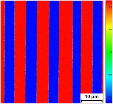
Product Description
Test pattern PFM03 is intended for:
・setting of the Piezoresponse Force Microscopy (PFM) mode, ・optimization of the modulation voltage parameters (frequency, phase and amplitude),
・test measurements in the PFM mode.
Sample description
Lithium niobate (LiNbO3) single-crystalline 500-μm-thick plate with roughness less than 10 nm cut normal to the polar axis.
A regular domain structure with period D was created in the sample. The spontaneous polarization has the opposite direction in the neighboring domains. The polarization direction determines the sign of piezoelectric coefficient. Analysis of the local piezoelectric response during application of the modulation voltage allows to reveal the domain pattern.
Specification
・Sample size – 5x5 mm
・Sample thickness, h – 500 μm
・Period, D – 10 μm
・Dash length, L – 100 μm
・Fixed on a metal substrate by conductive epoxy.
TERS
TERS — Raman Spectroscopy with the enhancement of the tip. Measurements based on AFM microscopy. Mode TERS Raman spectrum is enhanced when a sharp tip with a gold coating approaches the illuminated sample surface. Using the cantilever of an AFM as an amplifier, measure the chemical properties of the sample in the nano-range by using the built-in Raman spectrometer, simultaneously obtaining topographic data by using ASM.